63
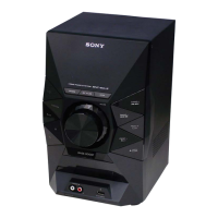
HCD-HX3/HX5/HX7
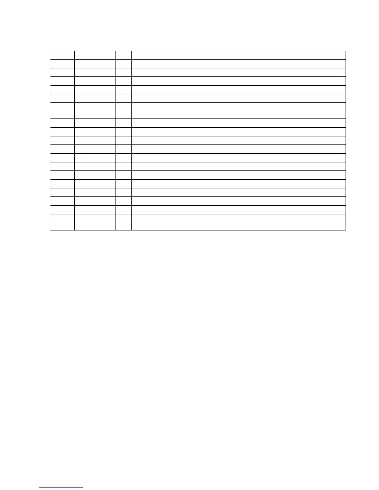
SWITCHING POWER BOARD IC11 CXD9841P (POWER CONTROL)
Pin No. Pin Name I/O Description
1
VSENSE I AC line voltage detection signal input terminal
2
F/B I Feed back signal input terminal for frequency modulation of oscillator
3
CT I Connected to the external capacitor for oscillator duty/frequency setting
4
RT I Connected to the external resistor for oscillator frequency setting
5
GND - Ground terminal
6
PROTECT I
Connected to the external capacitor for determines intermittent operation period when abnormal
detection state
7
SS I Connected to the external capacitor for soft start timing
8
VC1 I Power supply terminal for control circuit "L": stop
9 OCP I
Over current detection signal and didt protection signal input terminal
10
VC2 O Power supply output terminal for driver
11
P-GND - Ground terminal for low voltage side driver
12 VG (L)
OLow voltage side driver drive signal output terminal
13
--Not used
14
VB O Power supply output terminal for high voltage side driver
15
VS
I
High voltage side driver reference voltage input terminal
16 VG (H)
OHigh voltage side driver drive signal output terminal
17
--Not used
18
VD I
Terminal for drain-kick starting
When starting, current is supplied directly from the rectification diode to VC1
 Loading...