specified level : • —————— × 100 = less than ± 7%
• A+B= 300 ± 100 mVp-p
6. Remove the lead wire connected in step 1.
Focus/Tracking Gain Adjustment (RV102, RV103)
This gain has a margin, so even if it is slightly off. There is no prob-
lem.
Therefore, do not perform, this adjustment.
Please note that it should be fixed to mechanical center position
when you moved and do not know original position.
Adjustment Location :
[BD (CD) BOARD] – Side B –
2 (A+B)
A–B
A
B
symmetry
within 2.4
±
0.7 Vp-p
6. After check, remove the lead wire connected in step 2.
Note : • Try to measure several times to make sure that the ratio
of A : B or B : A is more than 10 : 7.
• Take sweep time as long as possible and light up the
brightness to obtain best waveform.
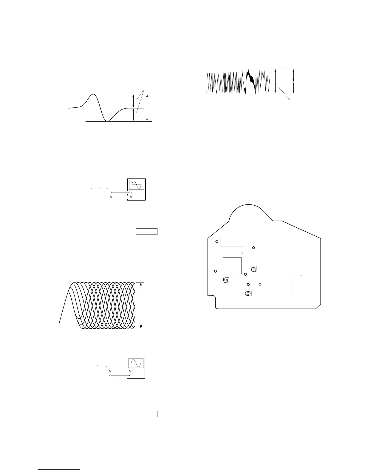
RF Level Check
+
–
BD (CD) board
TP (RF)
TP (VC)
oscilloscope
Procedure :
1. Connect oscilloscope to test point TP (VC) and TP (RF) on BD
(CD) board.
2. Turned Power switch on.
3. Put disc (YEDS-18) in and press the · (CD) key.
4. Confirm that oscilloscope waveform is clear and check RF sig-
nal level is correct or not.
Note :
Clear RF signal waveform means that the shape “≈” can be
clearly distinguished at the center of the waveform.
RF signal waveform
E-F Balance (Traverse) Check
Procedure :
1. Connect the TP (TEI) and TP (VC) with lead wire.
2. Connect oscilloscope to test point TP (VC) and TP (TEO) on
BD (CD) board.
3. Turned Power switch on.
4. Put disc (YEDS-18) in and press the · (CD) key.
5. Confirm that the oscilloscope waveform is symmetrical on the
top and bottom in relation to 0 Vdc, and check this level.
VOLT/DIV: 200 mV
TIME/DIV: 500 ns
level: 1.3
±
0.3Vp-p
+
–
BD (CD) board
TP (TEO)
TP (VC)
oscilloscope
(DC range)