– 119 –
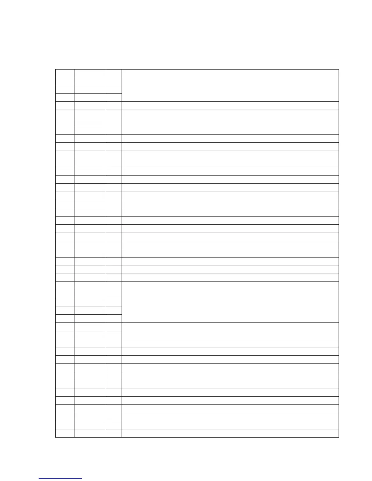
1—O
2 — O Not used (Open).
3—O
4 GND — AD converter ground
5
JOGGUIDE.TOP.
O JOG LED output
6
JOGGUIDE.ENT.
O ENTER LED output
7 AVREF1 — DA converter reference voltage input
8 RXD I Communication with the MD mechanism controller. Reception data input.
9 TXD O Communication with the MD mechanism controller. Reception data output.
10 CTS I Communication with the MD mechanism controller. Transmission request input from the other party.
11 RTS O Communication with the MD mechanism controller. Transmission request output.
12 FL.DATA O Data output to M66004.
13 FL.CLK O Clock output to M66004.
14 FL.CS. 1 O Chip select 1 of M66004
15 FL.CS. 2 O Chip select 2 of M66004
16 FL.RST O Reset output of M66004
17 MD RST I/O Forced reset output to the MD mechanism controller.
18 ATT O – 6 dB attenuate control of the MD analog input
19 DG2 O Green LED output of CD DISC2
20 DO2 O Orange LED output of CD DISC2
21 DG3 O Green LED output of CD DISC3
22 DO3 O Orange LED output of CD DISC3
23 DO1 O Orange LED output of CD DISC1
24 DG1 O Green LED output of CD DISC1
25 — O Not used (Open).
26 CD RESET O Reset output to the CD microprocessor
27 Y-D0 I/O
28 Y-D1 I/O
Communication with the CD microprocessor (Data input/output)
29 Y-D2 I/O
30 Y-D3 I/O
31 ST-SPEC1 I
Destination discrimination port for ST
32 ST-SPEC2 I
33 VSS — Ground
34 ST-SPEC3 I Destination discrimination port for ST
35 — I Not used (Connected to ground).
36 SYS.POWER O Power control output port
37 TA MUTE O TA mute output
38
JOGGUIDE.CUR.
O Cursor LED output
39 GROOVE O GROOVE LED output
40 DBFB O DBFB LED output
41 MD DISC O MD DISC LED output
42 STEREO I ST STEREO input
43 TUNED I ST TUNED input
44 — I Not used (Connected to ground).
Pin No. Pin Name I/O Function
Panel B Board IC501 µPD78058GC-411-3B9 (System Control, Display Control)


 To Next Page