– 121 –
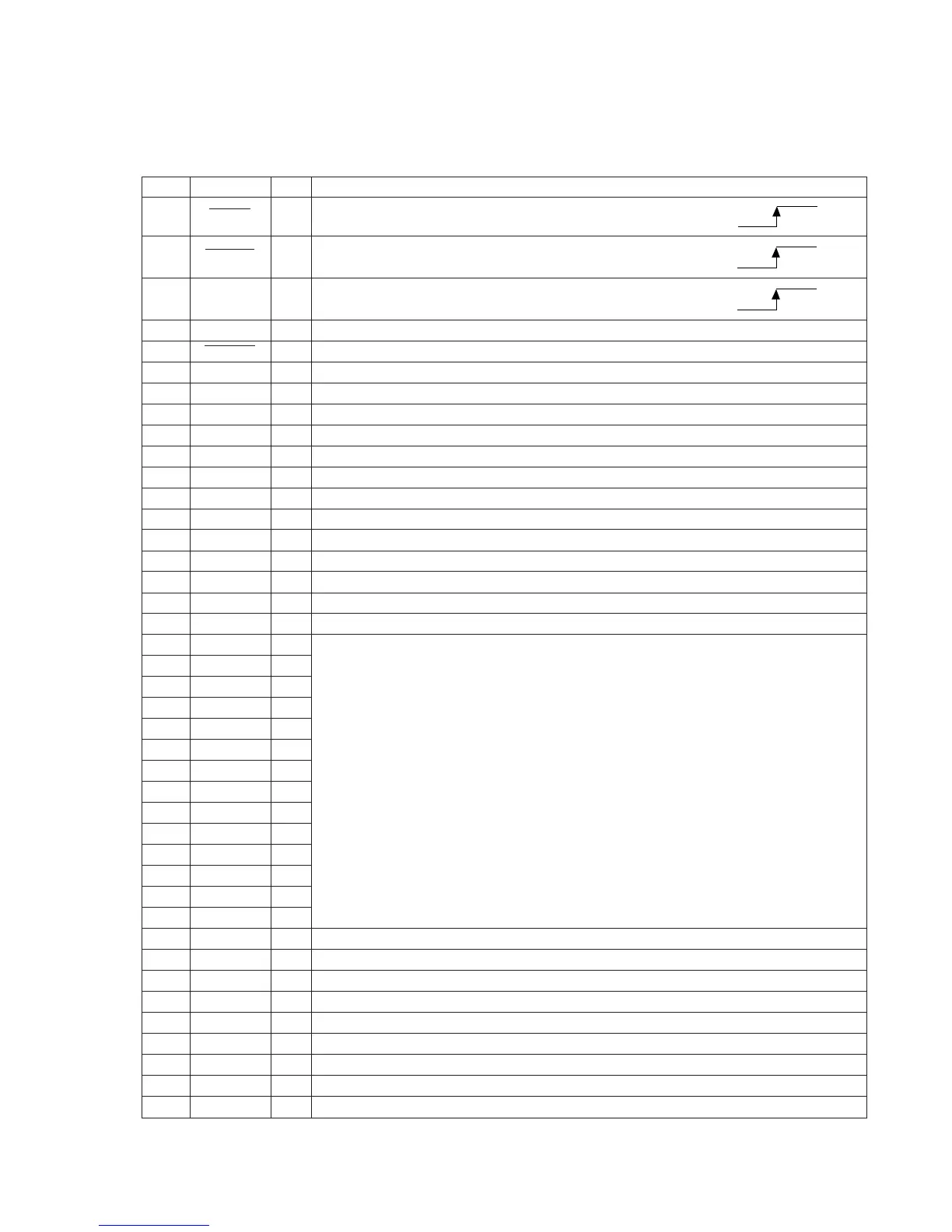
Pin No. Pin Name I/O Function
Relay Board IC851 µPD78055GC-055-3B9 (CD Mechanism Controller)
1 BDRST O BD reset output
2 A MUTE O Muting ON/OFF output. Not used (Open). Mute
3 FOCUSSW O Focus gain select output. Normal Down
4 AVSS — Ground potential of the A/D converter (Connected to VSS.)
5 DRVRST O M66004 reset output. Not used (Open).
6 — O Not used (Open).
7 AVREF1 I Reference voltage input of the D/A converter
8 GND I Not used (Connected to ground).
9 DRV DAT O M66004 data output. Not used (Open).
10 DRV CLK O M66004 clock output. Not used (Open).
11 SUBQ I Subcode Q serial input from the CXD2507.
12 — O Not used (Open).
13 SQCLK O Subcode Q reading clock output to the CXD2507.
14 PRGL O Latch pulse output to the PCM1710.
15 XLT O Latch pulse output to the CXD2507 and PCM1782.
16 SENSE I Various status input from the CXD2507 and PCM1782.
17 DATA O Serial data output to the CXD2507 and PCM1782.
18 CLK O Serial clock output to the CXD2507 and PCM1782.
19 — I
20 — I
21 — I
22 — I
23 — I
24 — I
25 — I
Not used (Open).
26 — I
27 — I
28 — I
29 — I
30 — I
31 — I
32 — I
33 VSS — Ground
34 JOG0 I JOG0 input. Not used (Connected to ground).
35 JOG1 I JOG1 input. Not used (Connected to ground).
36 BUSD0 I/O Y-BUS data 0
37 BUSD1 I/O Y-BUS data 1
38 BUSD2 I/O Y-BUS data 2
39 BUSD3 I/O Y-BUS data 3
40 ENCORDE0 I Disc tray address detect encoder input 0
41 ENCORDE1 I Disc tray address detect encoder input 1
RESET
RU


 To Next Page