2323
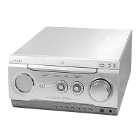
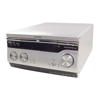
HCD-WZ8D
SECTION 4
DIAGRAMS
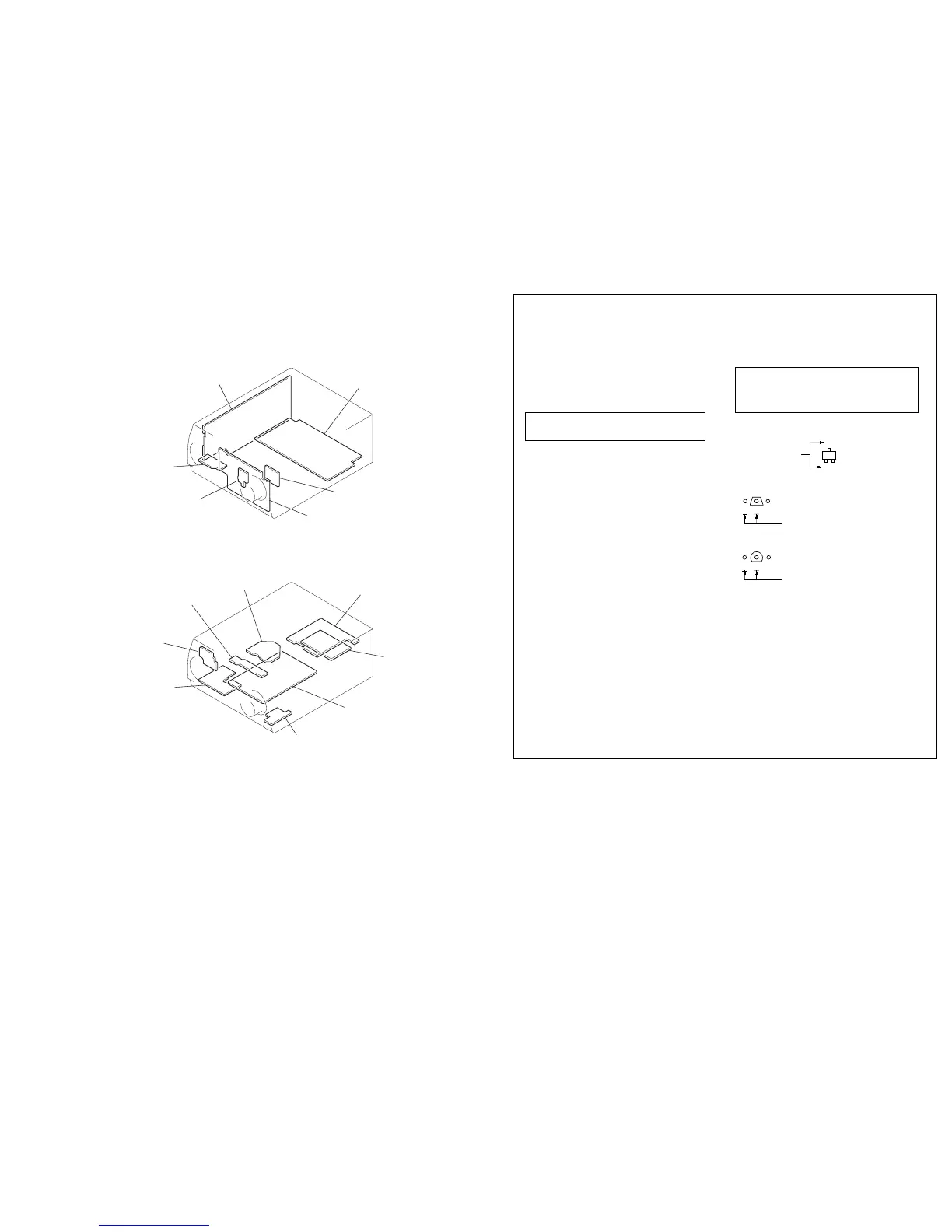
Circuit Boards Location
REGULATOR board
ENTER-SW board
CD-TC SW board
BACK LIGHT board
MAIN board
PANEL board
4CH-VOL board
DMB03 board
HP AMP board
MIC board
LCD board
MS-128 board
VIDEO board
RF board
Note on Schematic Diagram:
• All capacitors are in µF unless otherwise noted. pF: µµF
50 WV or less are not indicated except for electrolytics
and tantalums.
• All resistors are in Ω and
1
/
4
W or less unless otherwise
specified.
•
¢
: internal component
• 2 : nonflammable resistor
• 5 : fusible resistor
• C : panel designation
Note on Printed Wiring Boards:
• X : parts extracted from the component side
• Y : parts extracted from the conductor side
• b : Pattern from the side which enables seeing
• A : B+ Line
• B : B– Line
• H : adjustment for repair
•Power voltage is fed with DXA-WZ8D from external con-
nector (SYSTEM CONTROL 1, 2).
•Voltages and waveforms are dc with respect to ground
under no-signal (detuned) conditions.
•Voltages are taken with a VOM (Input impedance 10 MΩ).
Voltage variations may be noted due to normal produc-
tion tolerances.
•Waveforms are taken with a oscilloscope.
Voltage variations may be noted due to normal produc-
tion tolerances.
• Circled numbers refer to waveforms.
• Signal path
F : AUDIO
L : VIDEO
E : PB (TAPE)
a : REC (TAPE)
J : CD
c : DVD
d : TUNER
h : MD
N : Y
O : CHROMA
P : COMPONENT VIDEO
•Abbreviation
AUS: Australian model
E2 : 120V AC area in E model
E3 : 240V AC area in E model
E15 : 220-240V AC area in E model
EA : Saudi Arabia model
KR : Korean model
MY : Malaysia model
PH : Philippines model
RU : Russian model
SP : Singapore model
TH : Thai model
THIS NOTE IS COMMON FOR PRINTED WIRING BOARDS AND SCHEMATIC DIAGRAMS.
(In addition to this, the necessary note is printed in each block.)
C
B
These are omitted.
E
Q
B
These are omitted.
CE
Q
Note: The components identified by mark 0 or dotted line
with mark 0 are critical for safety.
Replace only with part number specified.
Caution:
Pattern face side: Parts on the pattern face side seen from
(SIDE B) the pattern face are indicated
Par ts face side: Parts on the parts face side seen from
(SIDE A) the parts face are indicated
• Indication of transistor
B
These are omitted.
CE
Q