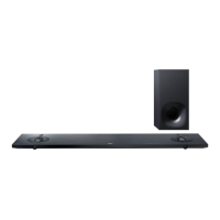
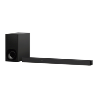
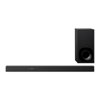
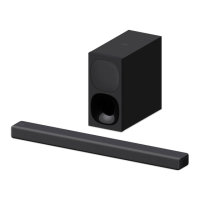
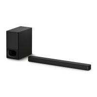
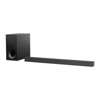
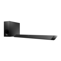
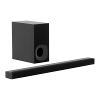
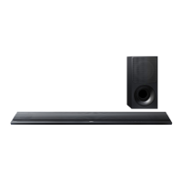
HT-NT3
HT-NT3
3131
For Schematic Diagrams.
Note:
• All capacitors are in μF unless otherwise noted. (p: pF) 50
WV or less are not indicated except for electrolytics and
tantalums.
• All resistors are in Ω and 1/4 W or less unless otherwise
specifi ed.
• Components for right channel have same values as for
left channel. Reference numbers are coded from
•
f
: Internal component.
• C : Panel designation.
THIS NOTE IS COMMON FOR PRINTED WIRING BOARDS AND SCHEMATIC DIAGRAMS.
(In addition to this, the necessary note is printed in each block.)
• A : B+ Line.
• Voltages and waveforms are dc with respect to ground
under no-signal conditions.
no mark
: POWER ON
• Voltages are taken with VOM (Input impedance 10 MΩ).
Voltage variations may be noted due to normal production
tolerances.
• Waveforms are taken with a oscilloscope.
Voltage variations may be noted due to normal production
tolerances.
• Circled numbers refer to waveforms.
• Signal path.
F : AUDIO (ANALOG)
J : AUDIO (DIGITAL)
E : VIDEO
d : LAN
G : WIRELESS LAN / BLUETOOTH
L : USB
• The voltage and waveform of CSP (chip size package)
cannot be measured, because its lead layout is different
from that of conventional IC.
For Printed Wiring Boards.
Note:
• X : Parts extracted from the component side.
• Y : Parts extracted from the conductor side.
•
f
: Internal component.
• : Pattern from the side which enables seeing.
(The other layers’ patterns are not indicated.)
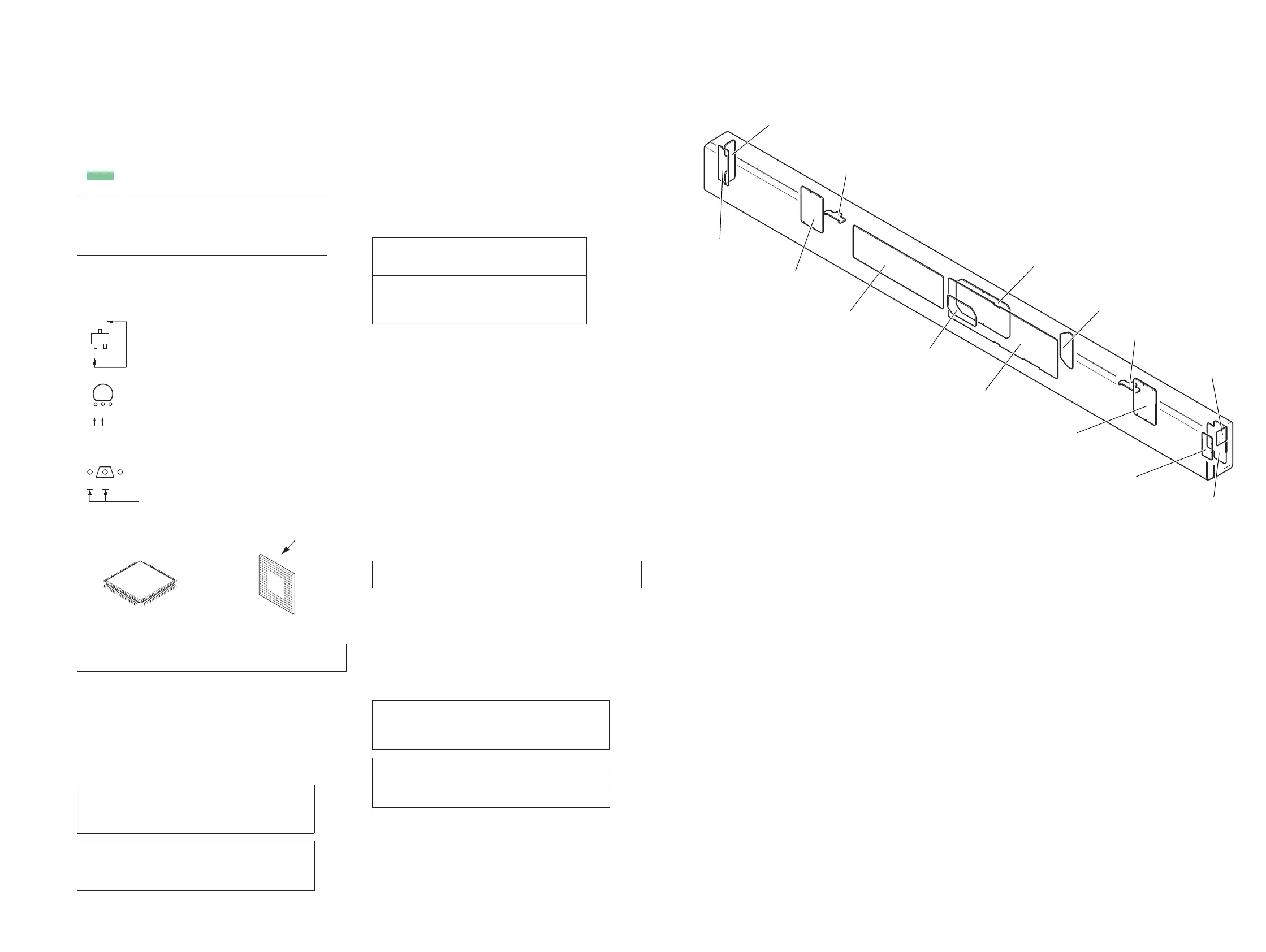
• Circuit Boards Location
• Indication of transistor.
C
B
These are omitted.
E
Q
CEB
These are omitted.
B
These are omitted.
CE
Q
Caution:
Pattern face side:
(Conductor Side)
Parts face side:
(Component Side)
Parts on the pattern face side seen
from the pattern face are indicated.
Parts on the parts face side seen from
the parts face are indicated.
• Abbreviation
AUS : Australian model
CND : Canadian model
E3 : 240V AC area in E model
EA : Saudi Arabia model
LA9 : Latin-American model
RU : Russian model
SP : Singapore model
TW : Taiwan model
• Abbreviation
AUS : Australian model
CND : Canadian model
E3 : 240V AC area in E model
EA : Saudi Arabia model
LA9 : Latin-American model
RU : Russian model
SP : Singapore model
TW : Taiwan model
• MB-1407 board is multi-layer printed board. However, the
patterns of intermediate layers have not been included in
diagrams.
MB-1407 board
OLED CHUKEI board
WS CHUKEI boar
REGULATOR, SWITCHING (3L405W)
CARD WLAN/BT COMBO
AMP board
IR TXR board
AUDIO IO board
RC-S730 (WW)
IR TXL board
KEY board
MOUNTED PWB (left)
MOUNTED PWB (right)
RF MODULATOR
(WS001)
Note: The components identifi ed by mark 0 or
dotted line with mark 0 are critical for safety.
Replace only with part number specifi ed.
Note: Les composants identifi és par une marque
0 sont critiques pour la sécurité.
Ne les remplacer que par une piéce portant
le numéro spécifi é.
• Lead layouts
surface
CSP (Chip Size Package) Lead layout of conventional IC
* Replacement of IC102 and IC103 on the MB1306 board used
in this unit requires a special tool.
* Replacement of IC102 and IC103 on the MB1306 board used
in this unit requires a special tool.
Note 1: When the complete AMP board is replaced, re-
fer to “NOTE OF REPLACING THE IC6001 ON
THE AMP BOARD AND THE COMPLETE AMP
BOARD” on page 5.
Note 1: When the complete AMP board is replaced, re-
fer to “NOTE OF REPLACING THE IC6001 ON
THE AMP BOARD AND THE COMPLETE AMP
BOARD” on page 5.
Note 2: When the C6078 and C6079 on the AMP board
are replaced, spread the bond referring to
“BOND FIXATION OF ELECTRIC PARTS” on
page 5.
Note 2: When the C6078 and C6079 on the AMP board
are replaced, spread the bond referring to
“BOND FIXATION OF ELECTRIC PARTS” on
page 5.
Ver. 1.1
 Loading...