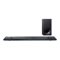
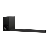
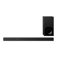
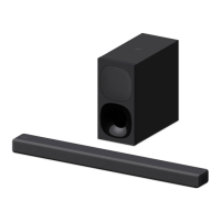
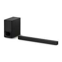
HT-NT3
63
Pin No. Pin Name I/O Description
V7 DGND12_K - Ground terminal
V8 DDRVREF_B I Reference voltage (+0.75V) input terminal for SD-RAM
V10 DGND12_K - Ground terminal
V11 DVCC12_K - Power supply terminal (+1.2V)
V12 to V17 DGND12_K - Ground terminal
V18 DVCC12_K - Power supply terminal (+1.2V)
V19 DGND12_K - Ground terminal
V20 DVCC12_K - Power supply terminal (+1.2V)
V21 DVCC33_IO_4 - Power supply terminal (+3.3V)
V22 AVDD33_X - Power supply terminal (+3.3V)
V23 to V25
VOUTD2, VOUTD4,
VOUTD5
- Not used
V28 NC - Not used
W1, W2 NC - Not used
W3 DDRVCCIO1 - Power supply terminal (+1.5V)
W4, W5 NC - Not used
W6 NC - Not used
W8 DDRVCCIO1 - Power supply terminal (+1.5V)
W10 DVCC12_K - Power supply terminal (+1.2V)
W11, W12 DVCC12_K - Power supply terminal (+1.2V)
W13, W14 DVCC12_K - Power supply terminal (+1.2V)
W15, W16,
W18, W19
DVCC12_K - Power supply terminal (+1.2V)
W20 DGND12_K - Ground terminal
W25, W26 VOUTD1, VOUTD0 - Not used
W27 NC - Not used
W28 USB_VRT_P2 - External reference resistor connection terminal
Y3, Y4 NC - Not used
Y7 DDRVCCIO1 - Power supply terminal (+1.5V)
Y18 DGND12_K - Ground terminal
Y20 AVSS33_COM - Ground terminal
Y22 AVSS33_USB_P2 - Ground terminal
Y23 DGND12_K - Ground terminal
Y26 AVDD33_USB_P2 - Power supply terminal (+3.3V)
AA1 NC - Not used
AA2 NC - Not used
AA3, AA4 NC - Not used
AA5 NC - Not used
AA6 NC - Not used
AA7 DGND12_K - Ground terminal
AA15 DDRVREF_D I Reference voltage (+0.75V) input terminal for SD-RAM
AA17 DDRVCCIO1 - Power supply terminal (+1.5V)
AA18 DGND12_K - Ground terminal
AA22 AVSS33_LD - Ground terminal
AA24 AVDD33_LD - Power supply terminal (+3.3V)
AA25 AVDD33_COM - Power supply terminal (+3.3V)
AA27 USB_DP_P2 I/O Two-way USB serial data (+) with the WLAN/BT COMBO card
AA28 USB_DM_P2 I/O Two-way USB serial data (-) with the WLAN/BT COMBO card
AB1 NC - Not used
AB2 NC - Not used
AB3 DDRVCCIO1 - Power supply terminal (+1.5V)
AB4 to AB6 NC - Not used
AB8, AB9 DGND12_K - Ground terminal
AB11 DDRVCCIO1 - Power supply terminal (+1.5V)
 Loading...