3
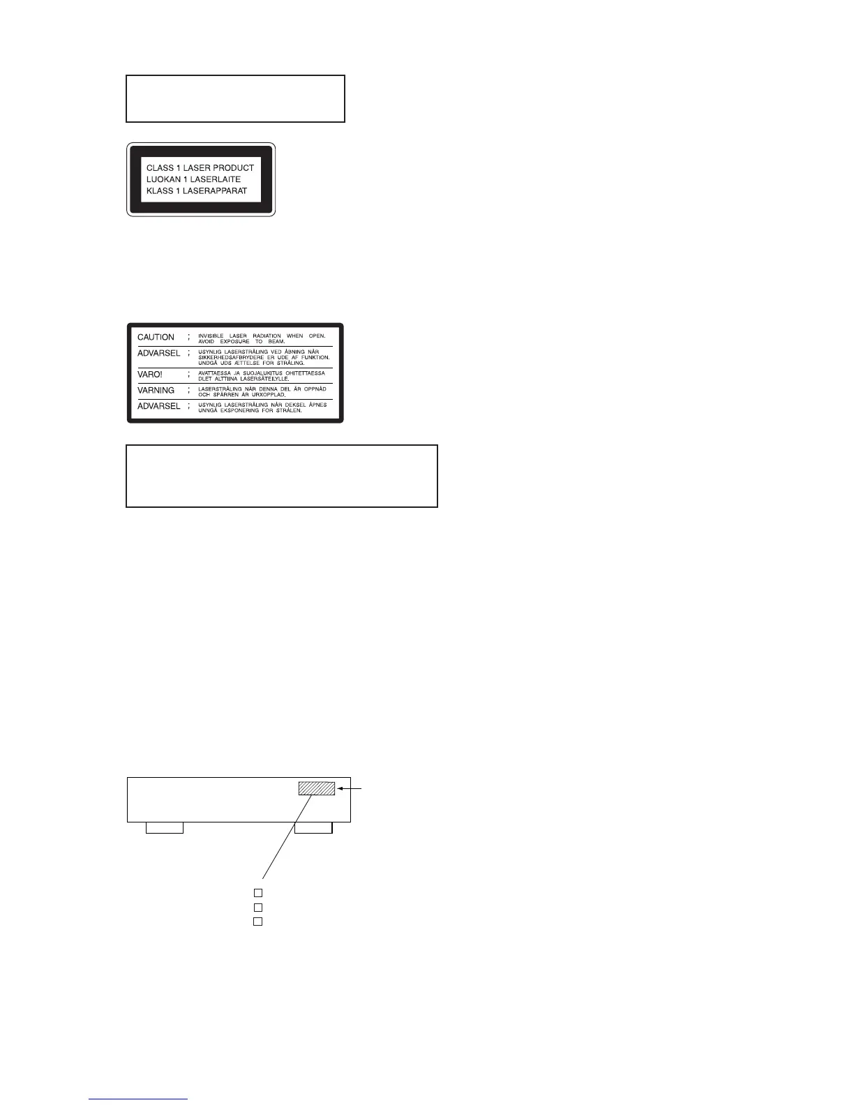
This appliance is classified as a CLASS 1 LASER product. The
CLASS 1 LASER PRODUCT MARKING is located on the rear
exterior.
The following caution label is located inside the unit.
Laser component in this product is capable
of emitting radiation exceeding the limit for
Class 1.
CAUTION
Use of controls or adjustments or performance of procedures
other than those specified herein may result in hazardous radiation
exposure.
Notes on chip component replacement
• Never reuse a disconnected chip component.
• Notice that the minus side of a tantalum capacitor may be
damaged by heat.
Flexible Circuit Board Repairing
• Keep the temperature of soldering iron around 270˚C
during repairing.
• Do not touch the soldering iron on the same conductor of the
circuit board (within 3 times).
• Be careful not to apply force on the conductor when soldering
or unsoldering.
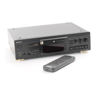
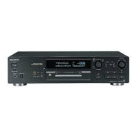
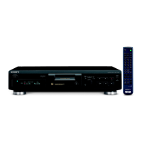
MODEL IDENTIFICATION
— BACK PANEL —
Parts No.
4-228-930-1 : AEP, UK model
4-228-930-2 : US model
4-228-930-3 : Canadian model
TABLE OF CONTENTS
1. SERVICING NOTE ·························································· 6
2. GENERAL ········································································ 12
3. DISAssembly
3-1. Case ·················································································· 16
3-2. Loading Panel ··································································· 16
3-3. Front Panel Assembly ······················································· 17
3-4. MD Mechanism Deck ······················································ 17
3-5. Tray Assembly ·································································· 18
3-6. BU Holder Assembly························································ 19
3-7. Motor (Loading) Assembly (M10) ··································· 19
3-8. Base Unit (MBU-5J) ························································ 20
3-9. BD Board·········································································· 20
3-10. Over Light Head (HR901)················································ 21
3-11. Mini Disc Device (KMS-260B/J1N) ································ 21
4. TEST MODE ···································································· 22
5. ELECTRICAL ADJUSTMENTS ······························· 27
6. DIAGRAMS
6-1. Block Diagrams ································································ 37
Main Section····································································· 37
Display/Power Supply Section ········································· 38
6-2. Circuit Board Location ····················································· 39
6-3. Printed Wiring Board BD Section ·································· 40
6-4. Schematic Diagram BD Section (1/2) ··························· 41
6-5. Schematic Diagram BD Section (2/2) ··························· 42
6-6. Schematic Diagram BD Switch Section························ 43
6-7. Printed Wiring Board BD Switch Section ······················· 43
6-8. Printed Wiring Board AD Section ································ 44
6-9. Schematic Diagram AD Section···································· 45
6-10. Printed Wiring Board DIO Section ······························ 46
6-11. Schematic Diagram DIO Section ·································· 47
6-12. Printed Wiring Board DA Section ································· 48
6-13. Schematic Diagram DA Section··································· 49
6-14. Printed Wiring Board DIGITAL Section ······················· 50
6-15. Schematic Diagram DIGITAL Section ························ 51
6-16. Schematic Diagram HP Section ··································· 52
6-17. Printed Wiring Board HP Section ································ 53
6-18. Schematic Diagram POWER Section ·························· 54
6-19. Printed Wiring Board POWER Section························ 55
6-20. Printed Wiring Board PANEL Section ························· 56
6-21. Schematic Diagram PANEL Section ···························· 57
6-22. Printed Wiring Board AC Section ································ 58
6-23. Schematic Diagram AC Section ··································· 59
6-22. IC Block Diagrams ··························································· 61
6-23. IC PinFunction Description ·············································· 66
7. EXPLODED VIEWS
7-1. Upper Case Assembly ······················································ 73
7-2. Front Panel Assembly ······················································· 74
7-3. Chassis Assembly ····························································· 75
7-4. Mechanism Deck Assembly-1 (MDM-6J) ······················· 76
7-5. Mechanism Deck Assembly-2 (MDM-6J) ······················· 77
7-6. Base Unit (MBU-5J) ························································ 78
8. ELECTRICAL PARTS LIST ······································· 79
 Loading...