SERVICE MANUAL
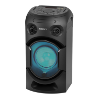
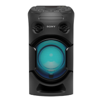
MHC-V21/V21D
MHC-V21/V21D
1
Note: The components identifi ed by mark 0 or
dotted line with mark 0 are critical for safety.
Replace only with part number specifi ed.
Note: Les composants identifi és par une marque
0 sont critiques pour la sécurité.
Ne les remplacer que par une pièce portant
le numéro spécifi
é.
SECTION 1
DIAGRAMS
SUPPLEMENT-1
MHC-V21/V21D
Subject: Addition of Schematic Diagram for SMPS board
File this supplement with the service manual.
Ver. 1.1 2018.08
9-890-697-81
US Model
Canadian Model
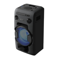
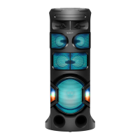
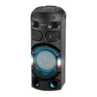
MHC-V21
AEP Model
UK Model
E Model
Australian Model
MHC-V21D
Note on Schematic Diagram:
• All capacitors are in μF unless otherwise noted. (p: pF)
50 V or less are not indicated except for electrolytics
and tantalums.
• All resistors are in and
1
/4 W or less unless otherwise
specifi ed.
•
2
: nonfl ammable resistor.
• C : panel designation.
• A
: B+ Line.
• B : B– Line.
• H : Adjustment for repair.
• Voltage and waveforms are dc with respect to ground
under no-signal (detuned) conditions.
no mark : TUNER
• Voltages are taken with a VOM (Input impedance 10 MΩ).
Voltage variations may be noted due to normal production
tolerances.
• Waveforms are taken with a oscilloscope.
Voltage variations may be noted due to normal production
tolerances.
• Circled numbers refer to waveforms.
• Signal path.
L : USB
N : MIC
THIS NOTE IS COMMON FOR SCHEMATIC DIAGRAMS.
(In addition to this, the necessary note is printed in each block.)
SYSSET
2018/08/2821:56:45(GMT+09:00)