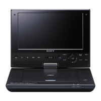
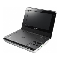
50
MV-700HR
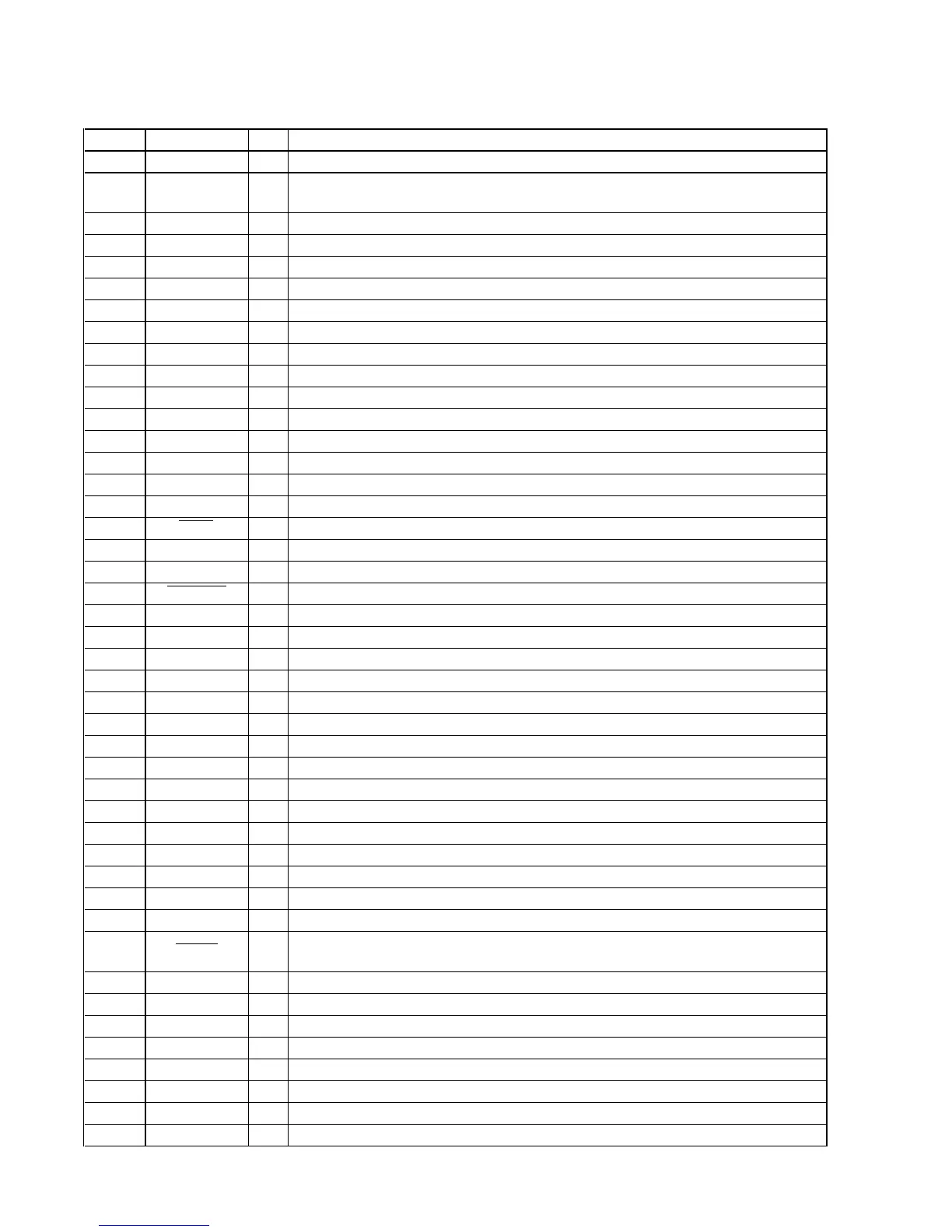
MONITOR BOARD IC401 µPD780024AGK-C85-9ET-A (SYSTEM CONTROLLER)
Pin No.
Pin Name I/O Description
1
TEST I Test mode setting terminal "H": test mode when power on, normally fixed at "L"
2
PW-ON O
Power on/off control signal output for main power and LED drive signal output
"H": power on, LED on
3
SHDN2 O Power on/off control signal output for the LCD (VSS -13V)
4
SHDN1 O Power on/off control signal output for the LCD (+7.5V)
5
NC O Not used
6
S-SCL O Serial data transfer clock signal output to the electrical volume
7
S-SDA I/O Serial data input/output to the electrical volume
8
MTRST O Reset signal output to the servo DSP
9
VSS0 - Ground terminal
10
VDD0 - Power supply terminal (+3.3V)
11
XIFCS O Chip select signal output to the servo DSP
12
XIFBUSY I Busy signal input from the servo DSP
13
*SDA I/O Two-way data bus with the TV tuner unit, EEPROM and real time clock IC
14
*SCL O Serial data transfer clock signal output to the TV tuner unit, EEPROM and real time clock IC
15
SIO I Serial data input from the servo DSP
16
SOO O Serial data output to the servo DSP
17
SCKO O Serial data transfer clock signal output to servo DSP
18
DOT SHIFT O Dot clock shift signal output to the clock generator circuit for OSD driver
19
OSD DATA O Serial data output to the OSD driver
20
OSD_CLK O Serial data transfer clock signal output to the OSD driver
21
TIMER_ON O Video control signal output terminal Not used
22
OSD_CS O Chip select signal output to the OSD driver
23
N/P O NTSC/PAL switching signal output terminal
24
VDD1 - Power supply terminal (+3.3V)
25
AVSS - Ground terminal
26
SYNC_DET I SYNC signal detection input terminal
27
KEY_DVD I Front panel key input terminal (A/D input)
28
KEY_IN I Monitor panel key input terminal (A/D input)
29
HOME CHECK I Cradle detection terminal "H": cradled
30
KEY_PW I Power key input terminal "L": power on
31
DST_SEL1 I Destination setting terminal
32
PW_DET I Battery voltage detection terminal
33
THRMAL I Temperature detection signal input terminal
34
AVREF I Reference voltage (+3.3V) input terminal
35
AVDD - Power supply terminal (+3.3V)
36
RESET I
System reset signal input from the reset signal generator or reset key "L": reset
For several hundreds msec. after the power supply rises, "L" is input, then it changes to "H"
37
XT2 - For system clock terminal Not used
38
XT1 - For system clock terminal Not used
39
FLASH I Internal flash memory data write control signal input terminal Not used
40
X2 O System clock output terminal (4.19 MHz)
41
X1 I System clock input terminal (4.19 MHz)
42
VSS1 - Ground terminal
43
VD I Vertical sync signal input from the RGB decoder
44
KEY_HALT I Wake up signal input from the power key
 Loading...