52
MV-700HR
MONITOR BOARD IC751
µ
PD6467GR-546-E1 (OSD DRIVER)
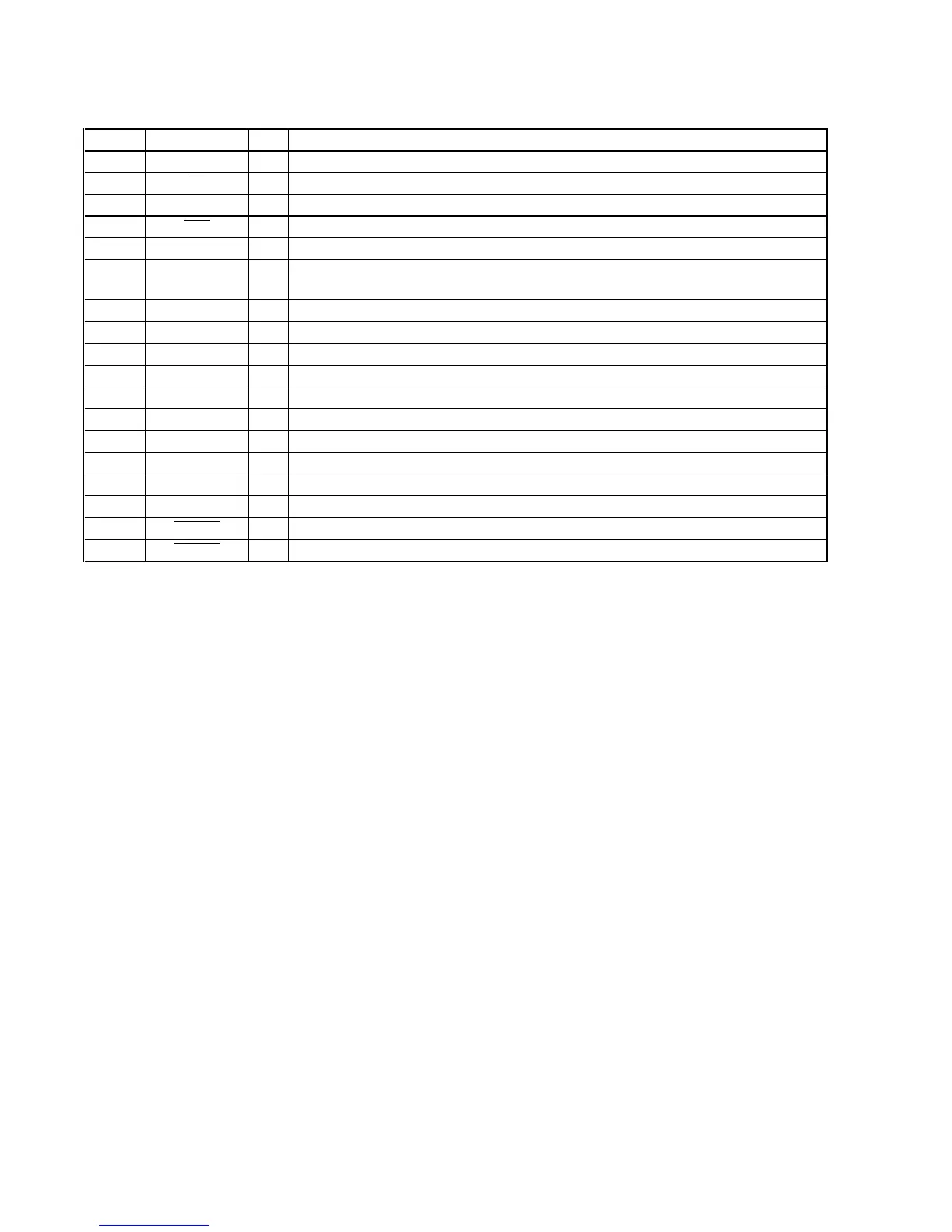
Pin No. Pin Name I/O Description
1 SCLK I
Serial data transfer clock signal input from the system controller
2CSI
Chip select signal input from the system controller
3 DATA I
Serial data input from the system controller
4 PCL I
Clear signal input after the power supply rises
5 VDD -
Power supply terminal (+3.3V)
6 CMDCT I
Command LSB/MSB first input selection signal input terminal
"L": LSB first, "H": MSB first Fixed at "H" in this set
7 OSC_OUT O
Output terminal from the clock generator circuit
8 OSC_IN I
Input terminal from the clock generator circuit
9
TEST
I
Test mode setting terminal "H": test mode, normally fixed at "L"
10 GND -
Ground terminal
11 BLK1 O
Blanking signal output terminal Not used
12 VC1 O
Character signal output terminal Not used
13 BLK2 O
Blanking signal output terminal Not used
14 VC2 O
Character signal output terminal Not used
15 VBLK O
Blanking signal output to the RGB decoder
16 to 18 VR, VG, VB O
Character signal output to the RGB decoder
19 VSYNC I
Vertical sync signal input from the RGB decoder
20 HSYNC I
Horizontal sync signal input from the LCD controller
 Loading...