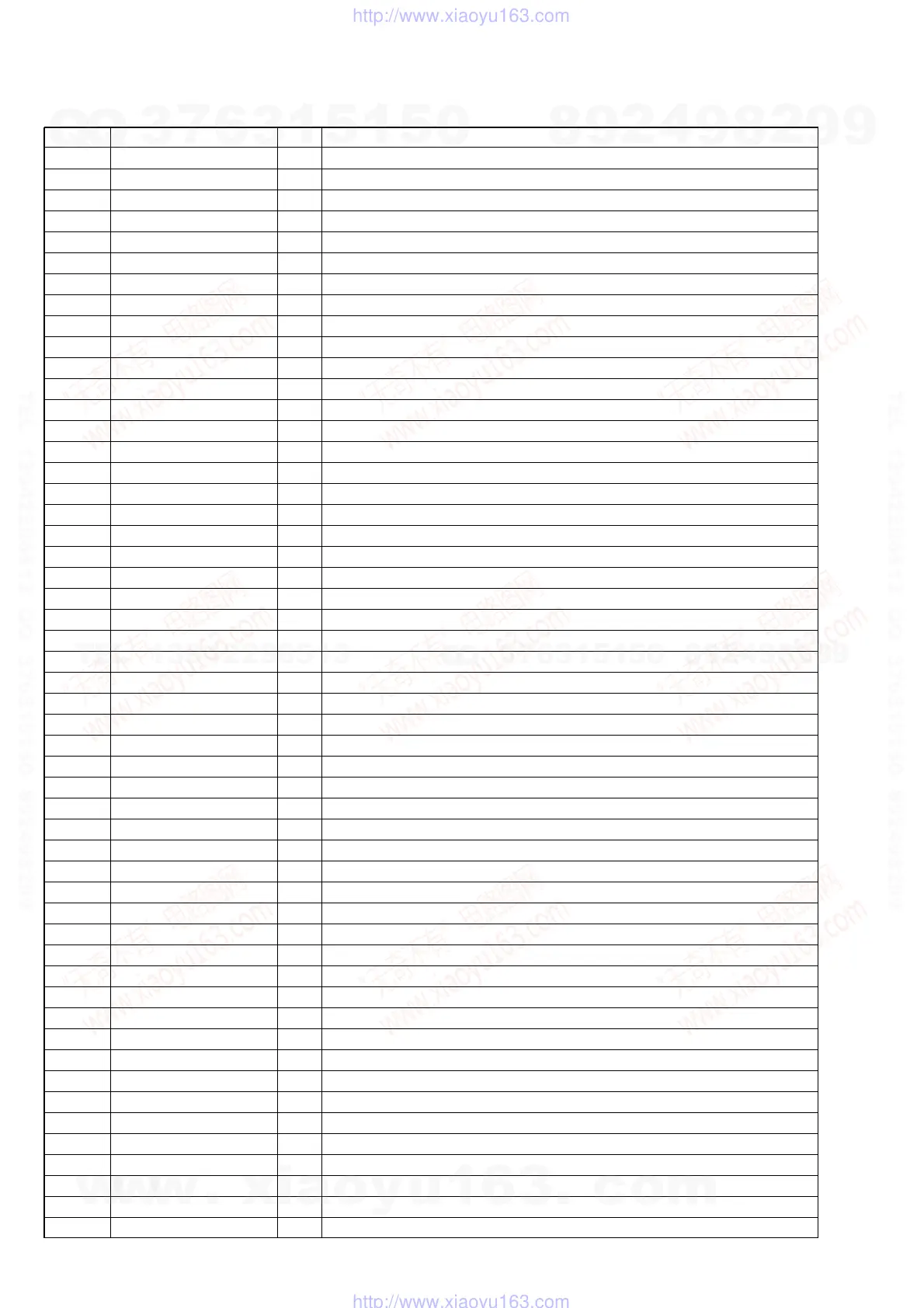
72
STR-DG910
IC3803 CXD9837R (PROGRESSIVE SCAN CONVERTER) (HDMI RE BOARD (4/4))
Pin No. Pin Name I/O Pin Description
1DVDD — Power supply pin (+3.3 V) (for I/O)
2CLKI I System clock signal input (27 MHz)
3 TEST17(PLL_TEST) I Test pin (Fixed at VSS in this set)
4 PLL_EN I PLL enable signal input
5, 6 P10, P11 I Video data input (Fixed at L in this set)
7 to 14 P12 to P19 I Video data input from video A/D converter.
15 NHSI I Horizontal sync signal input from video A/D converter.
16 NVSI I Vertical sync signal input from video A/D converter.
17 OVSS — Ground (for I/O)
18 THRM (IVSS) I Through mode setting terminal (Fixed at L in this set)
19 CVSS — Ground (for core)
20 NVSO O Vertical sync signal output for video encoder.
21 NHSO O Horizontal sync signal output for video encoder.
22 to 25 P09 to P06 O Video signal output (Not used in this set)
26 OVDD — Power supply pin (+3.3 V) (for I/O)
27 OVSS — Ground (for I/O)
28 to 33 P05 to P00 O Video signal output (Not used in this set)
34 TEST0 I Test pin (Fixed at L in this set)
35 OVSS — Ground (for I/O)
36 OVDD — Power supply pin (+3.3 V) (for I/O)
37 CVDD — Power supply pin (+2.5 V) (for core)
38 TEST1 I Test pin (Fixed at L in this set)
39 TEST2 I Test pin (Fixed at L in this set)
40 CLKO O System clock output (27 MHz) for video encoder.
41 to 45 Y09 to Y05 O Video signal output for video encoder.
46 OVDD — Power supply pin (+3.3 V) (for I/O)
47 OVSS — Ground (for I/O)
48 to 50 Y04 to Y02 O Video signal output for video encoder.
51, 52 Y01, Y00 O Video signal output (Not used in this set)
53 OVDD — Power supply pin (+3.3 V) (for I/O)
54 CVSS — Ground (for core)
55 OVSS — Ground (for I/O)
56, 57 C00, C01 O Video signal output (Not used in this set)
58 to 60 C02 to C04 O Video signal output for video encoder.
61 OVDD — Power supply pin (+3.3 V) (for I/O)
62 OVSS — Ground (for I/O)
63 to 67 C05 to C09 O Video signal output for video encoder.
68 FILM O Film sequence detection flag signal output (Not used in this set)
69 RFFI (W3IF) I MPEG flag (repeat first field flag) signal input (Fixed at L in this set)
70 OVSS — Ground (for I/O)
71 CVDD — Power supply pin (+2.5 V) (for core)
72 IVDD — Power supply pin (+3.3 V) (for I/O)
73 OVDD — Power supply pin (+3.3 V) (for I/O)
74 to 77 MD19 to MD16 I/O Two-way data bus input/output (Not used in this set)
78 OVDD — Power supply pin (+3.3 V) (for I/O)
79 OVSS — Ground (for I/O)
80 to 83 MA3, MA4, MA2, MA5 O Address signal output for SD-RAM.
84 OVDD — Power supply pin (+3.3 V) (for I/O)
85 OVSS — Ground (for I/O)
86 to 89 MA1, MA6, MA0, MA7 O Address signal output for SD-RAM.
90 OVSS — Ground (for I/O)
91 TEST5 (IVSS) — Ground (for I/O)
w
w
w
.
x
i
a
o
y
u
1
6
3
.
c
o
m
Q
Q
3
7
6
3
1
5
1
5
0
9
9
2
8
9
4
2
9
8
T
E
L
1
3
9
4
2
2
9
6
5
1
3
9
9
2
8
9
4
2
9
8
0
5
1
5
1
3
6
7
3
Q
Q
TEL 13942296513 QQ 376315150 892498299
TEL 13942296513 QQ 376315150 892498299
http://www.xiaoyu163.com
http://www.xiaoyu163.com