3
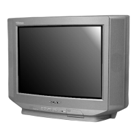
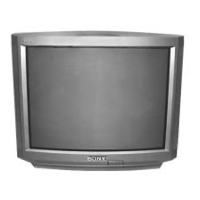
KV-21FK120
KV-21FK120
TABLE OF CONTENTS
SECTION TITLE PAGE
Specifi cations ............................................................................................................................................................................. 4
Warnings and Cautions .............................................................................................................................................................. 5
Safety Check-Out ....................................................................................................................................................................... 6
Self-Diagnostic Function ............................................................................................................................................................. 7
SECTION 1: DISASSEMBLY ............................................................................................................................................................. 9
1-1. Rear Cover Removal .......................................................................................................................................................... 9
1-2. Chassis Assembly Removal ............................................................................................................................................... 9
1-3. Service Position ............................................................................................................................................................... 10
1-4. Picture Tube Removal .......................................................................................................................................................11
Anode Cap Removal Procedure .......................................................................................................................................11
Wire Dressings ................................................................................................................................................................. 12
SECTION 2: SET-UP ADJUSTMENTS ............................................................................................................................................ 17
2-1. Beam Landing .................................................................................................................................................................. 17
2-2. Convergence .................................................................................................................................................................... 18
2-3. Focus ............................................................................................................................................................................... 19
2-4. Screen (G2) ...................................................................................................................................................................... 20
SECTION 3: SAFETY RELATED ADJUSTMENTS ......................................................................................................................... 21
3-1.
X
R565 Confi rmation Method (HV Hold-Down Confi rmation) and Readjustments ........................................................21
3-2. B+ Voltage Confi rmation and Adjustment ........................................................................................................................ 21
SECTION 4: CIRCUIT ADJUSTMENTS .......................................................................................................................................... 23
4-1. Remote Adjustment Buttons and Indicators ..................................................................................................................... 23
4-2. Accessing Service Adjustment Mode ............................................................................................................................... 23
4-3. White Balance Adjustments ............................................................................................................................................. 24
4-4. Memory Write Confi rmation Method ................................................................................................................................ 24
4-5. Service Data List .............................................................................................................................................................. 25
4-6. ID Map Table .................................................................................................................................................................... 33
4-7. A Board Adjustments ........................................................................................................................................................ 34
SECTION 5: DIAGRAMS ................................................................................................................................................................. 37
5-1. Circuit Boards Location .................................................................................................................................................... 37
5-2. Printed Wiring Board and Schematic Diagram Information .............................................................................................. 37
5-3. Block Diagram and Schematics ....................................................................................................................................... 38
A Board Schematic Diagram ............................................................................................................................................ 39
CV Board Schematic Diagram ......................................................................................................................................... 41
KR Board Schematic Diagram ......................................................................................................................................... 42
HK Board Schematic Diagram ......................................................................................................................................... 44
5-4. Semiconductors ............................................................................................................................................................... 45
SECTION 6: EXPLODED VIEWS .................................................................................................................................................... 46
6-1. Picture Tube ..................................................................................................................................................................... 46
6-2. Chassis ............................................................................................................................................................................ 47
SECTION 7: ELECTRICAL PARTS LIST ....................................................................................................................................... 48