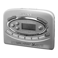
WM-FX522
1717
Note on Printed Wiring Board:
• X : parts extracted from the component side.
• Y : parts extracted from the conductor side.
• W : indicates side identified with part number.
•
f
: internal component.
• : Pattern from the side which enables seeing.
(The other layers' patterns are not indicated.)
6-3. NOTE FOR PRINTED WIRING BOARD AND SCHEMATIC DIAGRAMS
Note on Schematic Diagram:
• All capacitors are in µF unless otherwise noted. pF: µµF
50 WV or less are not indicated except for electrolytics
and tantalums.
• All resistors are in Ω and
1
/
4
W or less unless otherwise
specified.
•
f
: internal component.
• C : panel designation.
• A : B+ Line.
• H : adjustment for repair.
•Total current is measured with no cassette installed.
•Power voltage is dc 1.5V and fed with regulated dc power
supply from battery terminal.
•Voltages and waveforms are dc with respect to ground in
no-signal (detuned) conditions.
no mark : PLAYBACK
(): FM
〈〈 〉〉 : AM
•Voltages are taken with a VOM (Input impedance 10 MΩ).
Voltage variations may be noted due to normal produc-
tion tolerances.
•Waveforms are taken with a oscilloscope.
Voltage variations may be noted due to normal produc-
tion tolerances.
• Circled numbers refer to waveforms.
• Signal path.
F : FM
f : AM
E : PLAYBACK
•Waveforms
1 IC701 ua (XOUT)
2 IC801 5 (LX) (Playback mode)
3 Q405 (Collector) (FM/AM mode)
1.4 Vp-
306 ns
Caution:
Pattern face side: Parts on the pattern face side seen from
(Conductor Side) the pattern face are indicated.
Parts face side: Parts on the parts face side seen from
(Component Side) the parts face are indicated.
5 Q405 (Base) (FM/AM mode)
0.3 Vp-p
306 ns
 Loading...