24
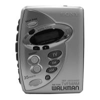
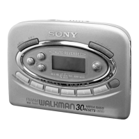
WM-FX522
Pin No. Pin Name I/O Description
68 RADIO ON O
Power on/off control signal output of the tuner circuit
“L”: power on (tuner on), “H”: power off (tape on)
69 NC O Not used
70
RESET I
System reset signal input “L”: reset
For several hundreds msec. after the power supply rises, “L” is input, then it changes to “H”
71 XOUT O Main system clock output terminal (75 kHz)
72 XIN I Main system clock input terminal (75 kHz)
73 GND — Ground terminal
74 VDB — Connection terminal of doubler circuit capacitor for liquid crystal display drive power supply
75, 76 C1, C2 —
Connection terminal of doubler circuit capacitor for liquid crystal display drive power supply
77 VEE —
Connection terminal of doubler circuit capacitor for liquid crystal display drive power supply
78, 79 C3, C4 —
Connection terminal of doubler circuit capacitor for liquid crystal display drive power supply
80 VLCD —
Connection terminal of doubler circuit capacitor for liquid crystal display drive power supply
 Loading...