EasyManua.ls Logo

ST STM32F405 Series User Manual

ST STM32F405 Series
50 pages
To Next Page IconTo Next Page
To Previous Page IconTo Previous Page
Page #18 background image
Reset and power supply supervisor AN4488
18/50 AN4488 Rev 7
power on/power down reset threshold, refer to the electrical characteristics in the product
datasheets.
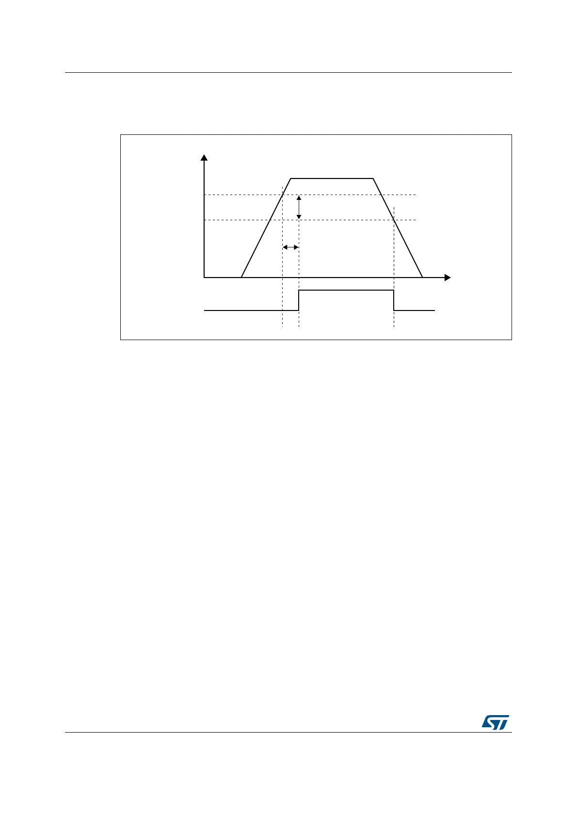
Figure 9. Power-on reset/power-down reset waveform
1. t
RSTTEMPO
is approximately 2.6 ms. V
POR/PDR
rising edge is 1.74 V (typ.) and V
POR/PDR
falling edge is
1.70 V (typ.). Refer to STM32F4xxxx datasheets for actual value.
The internal power-on reset (POR) / power-down reset (PDR) circuitry is disabled through
the PDR_ON pin. An external power supply supervisor should monitor V
DD
and should
maintain the device in reset mode as long as V
DD
is below a specified threshold. PDR_ON
should be connected to this external power supply supervisor. See
Section 3.2.1 for details.
3.2.3 Programmable voltage detector (PVD)
You can use the PVD to monitor the V
DD
power supply by comparing it to a threshold
selected by the PLS[2:0] bits in the Power control register (PWR_CR).
The PVD is enabled by setting the PVDE bit.
A PVDO flag is available, in the Power control/status register (PWR_CSR), to indicate
whether V
DD
is higher or lower than the PVD threshold. This event is internally connected to
EXTI Line16 and can generate an interrupt if enabled through the EXTI registers. The PVD
output interrupt can be generated when V
DD
drops below the PVD threshold and/or when
V
DD
rises above the PVD threshold depending on the EXTI Line16 rising/falling edge
configuration. As an example the service routine can perform emergency shutdown tasks.
6
$$
0/2
0$2
M6
HYSTERESIS
4EMPORIZATION
T
2344%-0/
2%3%4
AIB
6
0/20$2
FALLINGEDGE
6
0/20$2
RISINGEDGE

Table of Contents

Question and Answer IconNeed help?

Do you have a question about the ST STM32F405 Series and is the answer not in the manual?

ST STM32F405 Series Specifications

General IconGeneral
Core Size32-bit
Maximum CPU Clock Speed168 MHz
Flash Memory Size1 MB
RAM Size192 KB
ADC ChannelsUp to 16
DAC Channels2
I2C Interfaces3
SPI Interfaces3
CPU CoreARM Cortex-M4
Operating Voltage1.8 V to 3.6 V
TimersUp to 17
PeripheralsDMA, RTC, CRC
Operating Temperature-40°C to +85°C
Package / CaseLQFP, WLCSP

Summary

STM32F4 Power Supply Management

System Reset and Power Supervisor Circuits

System Reset Mechanisms and NRST Pin

Explains system reset events, sources, and the NRST pin functionality.

Power-On/Down Reset and Voltage Detection

Covers POR/PDR, PVD, and the role of the PDR_ON pin for power supply supervision.

STM32F4 Package Options and Selection

STM32F4 Boot Mode Configuration

Explanation of the three boot modes (Flash, System Memory, SRAM) selectable via BOOT pins.

STM32F4 Debugging Interfaces and Tools

SWJ Debug Port: Serial Wire and JTAG

Details on the Serial Wire/JTAG Debug Port (SWJ-DP) integrating JTAG and SW interfaces.

STM32F4 Clock Sources and Configuration

PCB Routing Guidelines for STM32F4 Devices

PCB Stack-up Design for High-Speed Signals

Guidance on designing PCB stack-ups for high-speed signals, including 4, 6, and 8-layer examples.

Frequently Asked Questions (FAQ) for STM32F4

Troubleshooting Common MCU Issues

Troubleshooting common root causes for MCU malfunction, such as power, reset, and boot pins.

Related product manuals