Package AN4488
22/50 AN4488 Rev 7
4.2 Pinout Compatibility
4.2.1 I/O speed
• When using the GPIO as I/O, design considerations have to be taken into account to
ensure that the operation is as intended.
• When the load capacitance becomes larger, the rise/fall time of the I/O pin increases.
This capacitance includes the effects of the board traces.
• I/O characteristics are available in the product’s datasheet.
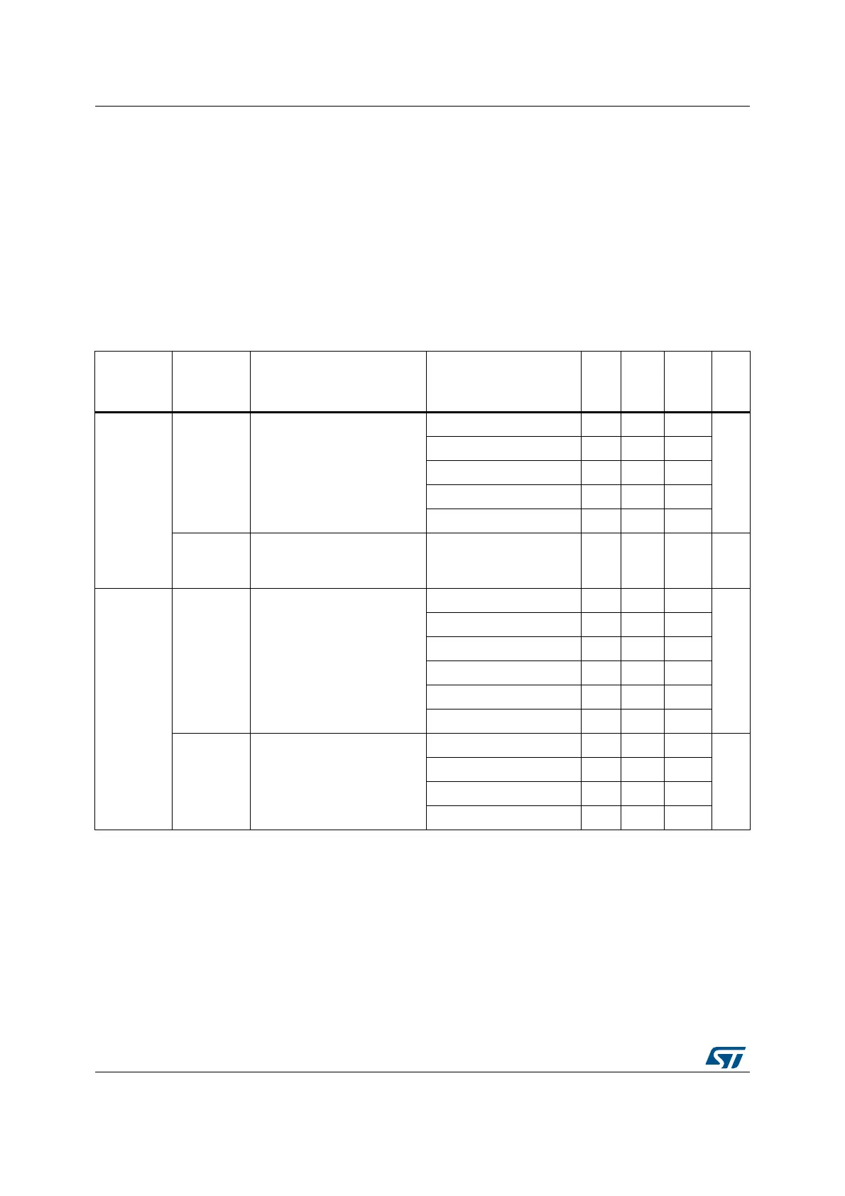
• Table 4 illustrates the I/O AC characteristics of the STM32F469xx:
Table 4. I/O AC characteristics
(1)(2)
OSPEEDR
y[1:0] bit
value
(1)
Symbol Parameter Conditions Min Typ Max Unit
00
f
max(IO)out
Maximum frequency
C
L
= 50 pF, V
DD
≥ 2.7 V - - 4
MHz
C
L
= 50 pF, V
DD
≥ 1.7 V - - 2
C
L
= 10 pF, V
DD
≥ 2.7 V - - 8
C
L
= 10 pF, V
DD
≥ 1.8 V - - 4
C
L
= 10 pF, V
DD
≥ 1.7 V - - 3
t
f(IO)out
/
t
r(IO)out
Output high to low level fall
time and output low to high
level rise time
C
L
= 50 pF, V
DD
= 1.7 V
to 3.6 V
--100ns
01
f
max(IO)out
Maximum frequency
(3)
C
L
= 50 pF, V
DD
≥ 2.7 V - - 25
MHz
C
L
= 50 pF, V
DD
≥ 1.8 V - - 12.5
C
L
= 50 pF, V
DD
≥ 1.7 V - - 10
C
L
= 10 pF, V
DD
≥ 2.7 V - - 50
C
L
= 10 pF, V
DD
≥ 1.8 V - - 20
C
L
= 10 pF, V
DD
≥ 1.7 V - - 12.5
t
f(IO)out
/
t
r(IO)out
Output high to low level fall
time and output low to high
level rise time
C
L
= 50 pF, V
DD
≥ 2.7 V - - 10
ns
C
L
= 10 pF, V
DD
≥ 2.7 V - - 6
C
L
= 50 pF, V
DD
≥ 1.7 V - - 20
C
L
= 10 pF, V
DD
≥ 1.7 V - - 10
 Loading...