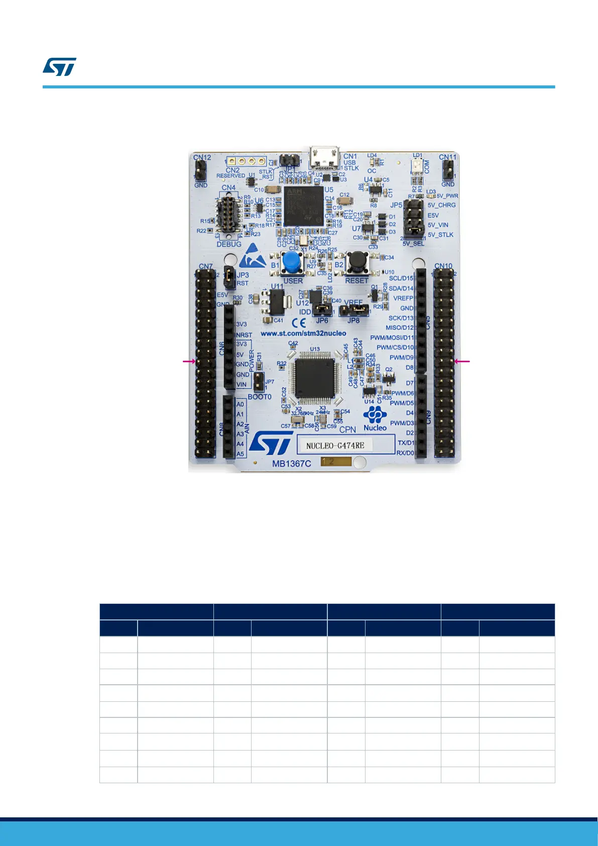
Figure 19. ST morpho connectors
CN7
MORPHO[1:38]
CN10
MORPHO[1:38]
The pinout of ST morpho connectors CN7 and CN10 is shown in Figure 18. Arduino
™
and ST morpho connectors
pinout.
Note: The D0 and D1 signals are connected by default to USART1 (MCU I/O PC4 and PC5). For details about how to
modify the UART interface, refer to Section 6.6.5 Virtual COM port (VCP): LPUART and USART.
Table 16 shows the pin assignment of each STM32G4 I/O on the ST morpho connector.
Table 16. Pin assignment of the ST morpho connectors
CN7 odd pins
CN7 even pins CN10 odd pins CN10 even pins
Pin nbr Pin name Pin nbr
Pin name
(1)
Pin nbr
Pin name
(1)
Pin nbr Pin name
1 PC10 2 PC11 1 PC9 2 PC8
3 PC12 4 PD2 3 PB8 4 PC6
5 VDD 6 E5V 5 PB9 6 PC5
7
BOOT0
(2)
8 GND 7
VREFP
(3)
8
5V_USB_CHGR
(4)
9 NC 10 NC 9 GND 10 NC
11 NC 12 IOREF 11 PA5 12 PA12
13
PA13
(5)
14 NRST 13 PA6 14 PA11
15
PA14
(5)
16 3V3 15 PA7 16 PB12
17 PA15 18 5V 17 PB6 18 PB11
UM2505
ST morpho connectors CN7 and CN10
UM2505 - Rev 2
page 32/43
 Loading...