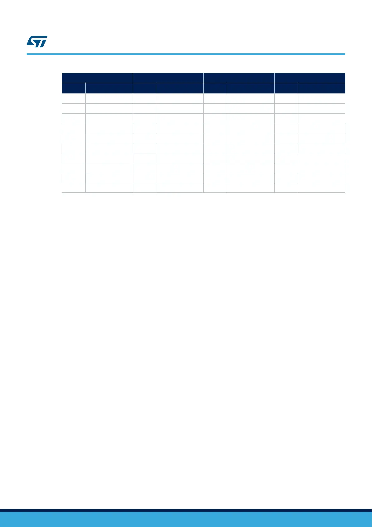
CN7 odd pins CN7 even pins CN10 odd pins CN10 even pins
Pin nbr Pin name Pin nbr
Pin name
(1)
Pin nbr
Pin name
(1)
Pin nbr Pin name
19 GND 20 GND 19 PC7 20 GND
21 PB7 22 GND 21 PA9 22 PB2
23 PC13 24 VIN 23 PA8 24 PB1
25 PC14 26 NC 25 PB10 26 PB15
27 PC15 28 PA0 27 PB4 28 PB14
29 PF0 30 PA1 29 PB5 30 PB13
31 PF1 32 PA4 31 PB3 32 AGND
33 VBAT 34 PB0 33 PA10 34 PC4
35 PC2 36 PC1/PB9 35 PA2 / PC4 36 NC
37 PC3 38 PC0/PA15 37 PA3 / PC5 38 NC
1. Default configuration in bold.
2. BOOT0 is not connected by default. The BOOT0 function is done by SW:
• Option byte nSWBOOT0 must be set to 0 (in that case, BOOT0 is taken from the Option byte nBOOT0)
• Option byte nBOOT0 must be set to 1 (in that case BOOT0 is active low).
If nSWBOOT0 is set to 0, the BOOT0 is taken from pin PB8 / BOOT0.
3. AVDD connected to VREF+
4. 5V_USB_CHGR is the 5 V power from the STLINK-V3E USB connector that rises first. It rises before the 5 V rising on the
board.
5. PA13 and PA14 are shared with SWD signals connected to STLINK-V3E. It is not recommended to use them as I/O pins.
UM2505
ST morpho connectors CN7 and CN10
UM2505 - Rev 2
page 33/43
 Loading...