UM0718 Getting started
Doc ID 15846 Rev 1 7/31
1.2.1 Configuring the hardware
The connectors must be configured correctly, as described in Tabl e 1 .
The user must connect the USB port of the PC or notebook to connect the demonstration
board. The demonstration board should also be connected with the compatible slave
module using the PMBus connector pins.
Table 1. Connectors
Connector
name
Description
USB
Connector
USB type B connector to communicate with the PC GUI
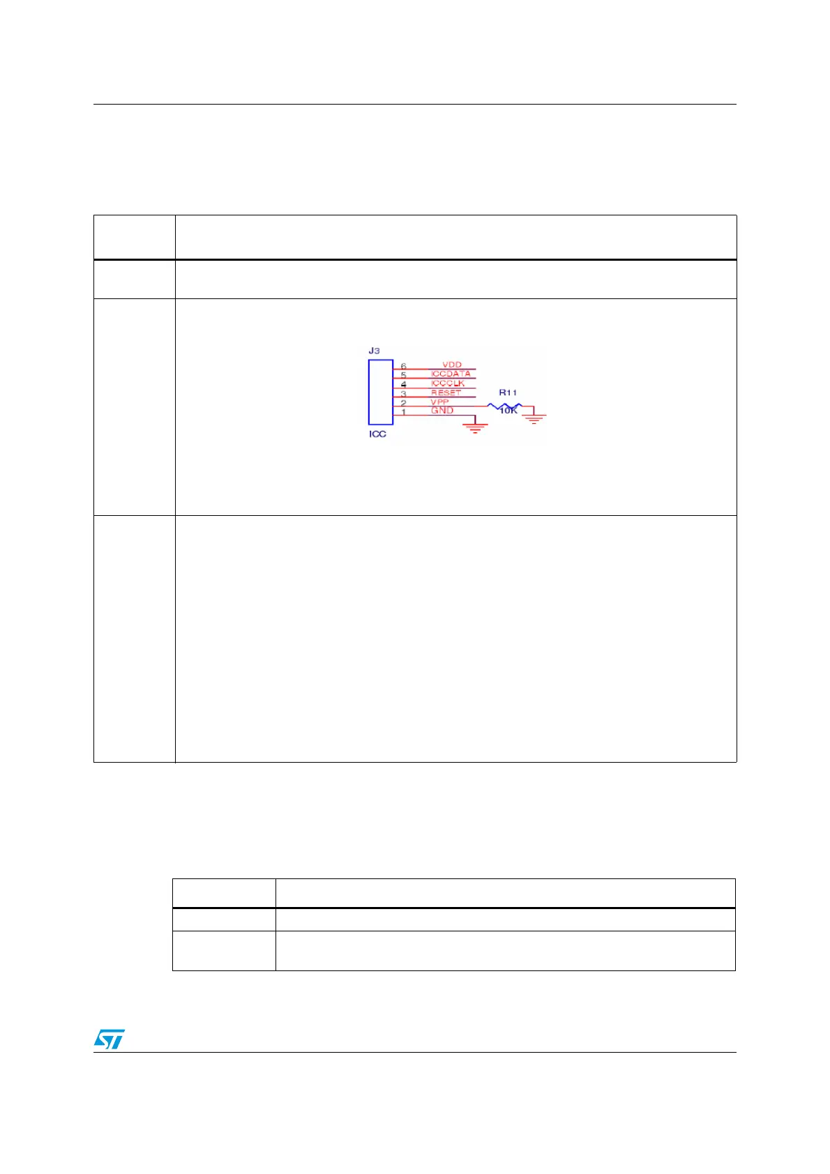
J3
ICC connector pins to re-program the MCU if needed. The connection is shown in the following
diagram:
Note: This 6-pin connection is a customized ICC connector from the normal
connector. This modification is performed to achieve the low-form factor of
the board.
J8 (PMBus)
The following is the 10-pin PMBus interface connector description:
– Pin 1: Control signal 5
– Pin 2: Control signal 4
– Pin 3: Control signal 3
– Pin 4: Control signal 2
– Pin 5: VDD_OUT. Refers to slide switch position.
– Pin 6: Ground
– Pin 7: Control signal 1
– Pin 8: PMBus alert signal coming from the slave device.
– Pin 9: PMBus clock signal. This signal is always driven by the MCU in this demonstration board.
– Pin 10: PMBus data signal. This signal is bi-directional.
Note: The voltage on the control lines is either 5 V or 0 V depending on the
selection made through the GUI.
Table 2. Switches
Switch name Description
SW1(Reset) The reset switch restarts the application
J9(EG1313)
The voltage on VDD_OUT can be varied (5 V/ 3.3 V/NC) by varying the slide
switch positions.