DWC ADC 12b5M SAR, TSMC180 IP Databook
April 2012 Synopsys, Inc. 25-30
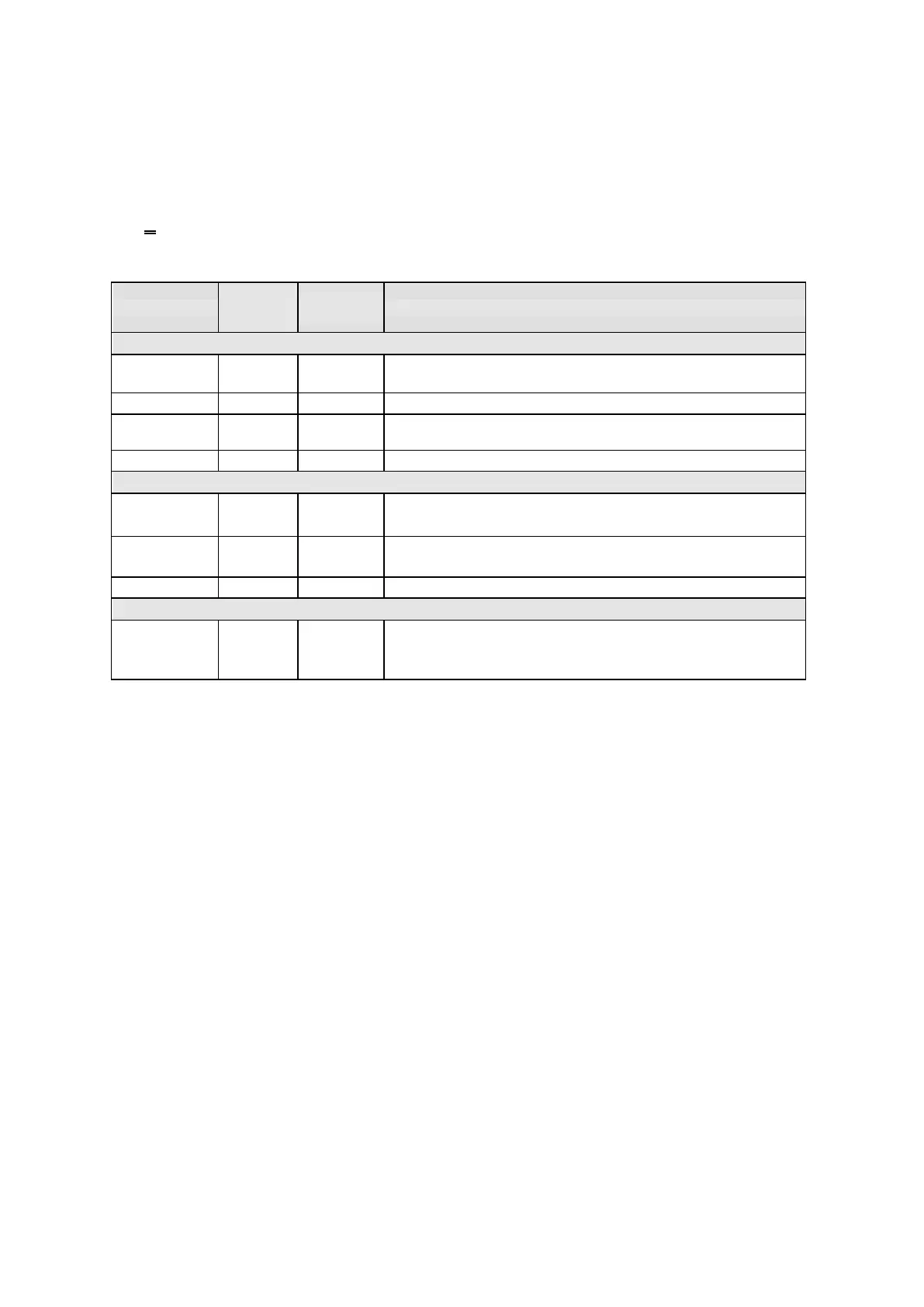
11 Cell Routing Constrains
The table below presents the signals whose routing must follow constrains.
Unless otherwise stated the analog signal shielding is made with each cell‟s agnd (or avdd
as 2
nd
option).
Table 4 – ADC signals with routing constrains
For full performance, the supply voltage at the boundary of the IP
must respect the range in databook‟s specification table.
For full performance, the supply voltage at the boundary of the IP
must respect the range in databook‟s specification table.
Shield from any digital signal.
Higher wire resistance increases the gain error.
Shield from any digital signal.
Higher wire resistance increases the offset error.
Load capacitance should be below 5pF
Shield from any digital signal and other vinX
Different routing between inputs may originate gain and offset
errors between channels
n.a. – Not Applicable