DWC ADC 12b5M SAR, TSMC180 IP Databook
April 2012 Synopsys, Inc. 8-30
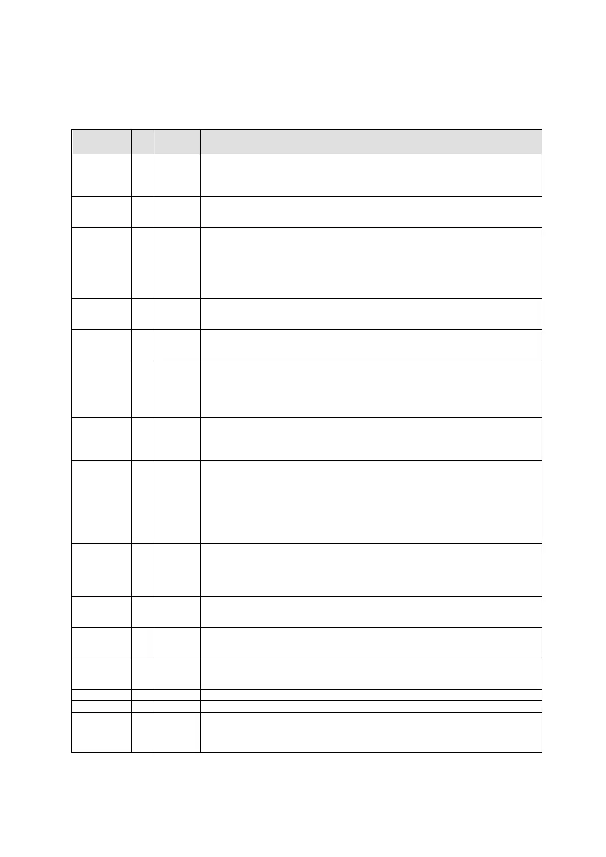
5 Pin Description
Analog input signals
In differential input mode (seldiff=H), vinp18...vinp1 are the positive inputs, vinn18...vinn1 are
the negative inputs.
vinp0 available only for single ended input mode.
Analog input signals
In single ended input mode (seldiff=L), the negative input vinn0 must be connected to
ground.
Positive Reference Voltage,
The reference voltage must be applied externally to the vrefp pin, in order to define the ADC
full scale input range.
This pin presents a sw itched capacitive load to its driver, that will be around 3pF in worst
case. The switching frequency is the clock frequency. The vrefp input impedance will vary
through the conversion cycle, between the described 3pF and a negligible capacitor value of
around 1fF.
Negative Reference Voltage
The reference ground voltage must be applied externally to the agndref pin, in order to define
the ADC full scale input range
Internal voltage regulator analog probing test signal.
Under ADC test mode it is mandatory to have direct access to this signal from chip pinout or
through registers.
Selects the ADC resolution:
selres=00 6-bit mode
selres=01 8-bit mode
selres=10 10-bit mode
selres=11 12-bit mode
Selects the ADC input mode (18 selectable inputs are available in both configurations,
vinp0|n0 is available only for single-ended mode):
seldiff=L single ended inputs
seldiff=H differential input
This digital input signal must have 3.3 V levels (avdd).
This signal is used for two purposes:
1. When there is no digital supply (dvdd) but the analog supply (avdd) it is powered on,
activating this signal (dislvl = H) prevents current consumption on analog supply (avdd)
during digital supply (dvdd) startup.
2. This signal is also used to control the power switching of dvdd inside the IP, defining the
deep power down mode.
Input multiplexer control signals:
- vinp|n0 selected when sel4..0=0H
- vinp|n18 selected when sel4..0=12H;
Under ADC test mode it is mandatory to have access to this signal, directly from chip pinout
or through registers.
Reset of internal buffers and registers (Active H).
Under ADC test mode it is mandatory to have direct access to this signal from chip pinout or
through registers.
Start-of -conversion signal (Active H). Starts the conversion cycle on the next clk rising edge.
Under ADC test mode it is mandatory to have direct access to this signal from chip pinout or
through registers.
Clock Input.
Under ADC test mode it is mandatory to have direct access to this signal from chip pinout or
through registers.
Enable ADC (enadc=H normal operation).
Enable internal voltage regulator (enldo=H normal operation).
Digital signals to enable internal analog programmability modes used for test purposes. In
normal operation these signals should be connected in to gnd.
Under ADC test mode it is mandatory to have access to this signal, directly from chip pinout
or through registers.