EasyManua.ls Logo

Synopsys TSMC180 - 4 Specifications; Analog Input and Biasing; Digital Output and Timing

Default Icon
30 pages
Print Icon
To Next Page IconTo Next Page
To Previous Page IconTo Previous Page
Loading...
DWC ADC 12b5M SAR, TSMC180 IP Databook
April 2012 Synopsys, Inc. 5-30
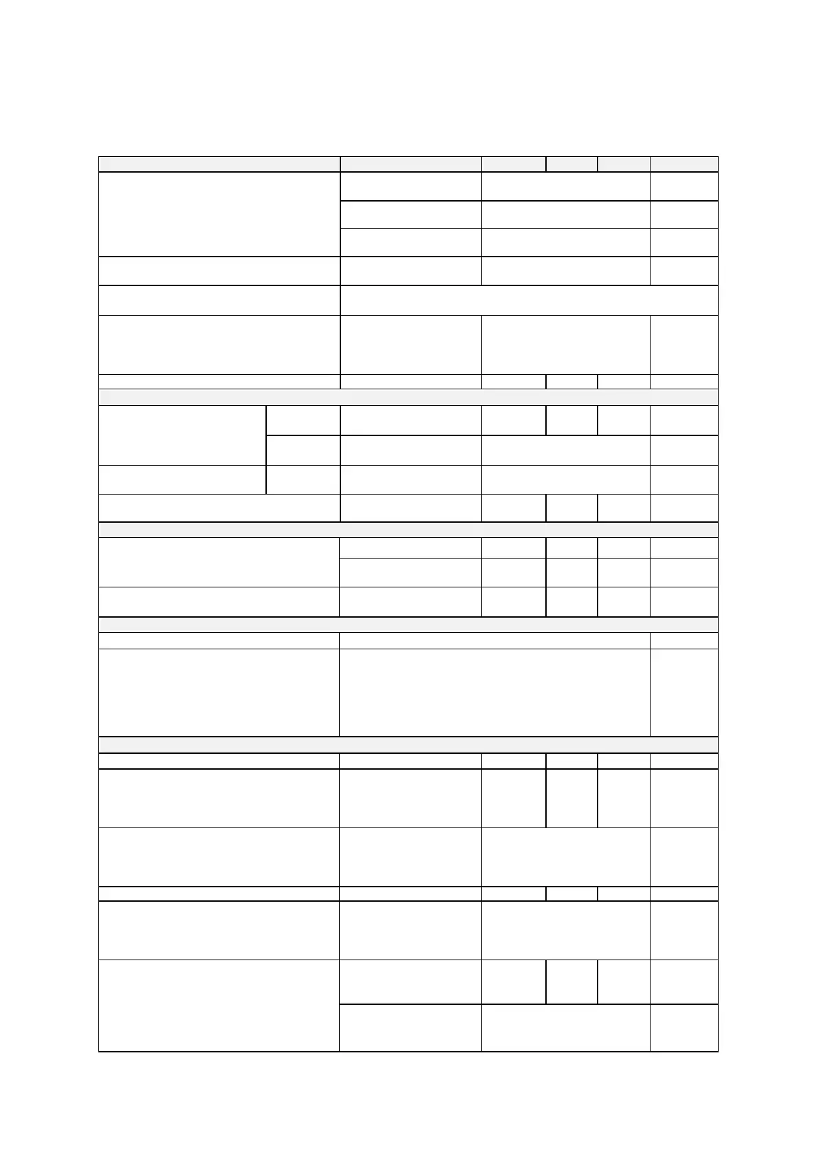
4 Specifications
Parameter
Conditions
MIN
TYP
MAX
Technology
No analog options
TSMC 180nm G CMOS, w ith
3.3V IO devices
Minimum metal stack
supported
5m_3x1n
Metal stack available in
DWDL
5m_3x1n , 6m_4x1n
Area
-
0.25
796 x 314
Standard Cell Library
(TSMC) TCB018GBWP7T Rev. 270a
TSMC 180nm Core Library
Resolution
selres=11
selres=10
selres=01
selres=00
12
10
8
6
Junction temperature
-
-40
+50
+125
Analog Input
Full-scale input range
seldiff=L
agndref
vrefp
seldiff=H
2*(vrefp agndref)
Input signal common mode
(only for differential mode)
seldiff=H
(vrefp + agndref)/2
Input sampling capacitance (C
S
)
1
No parasitic
capacitances included
5
Analog Biasing
Positive reference voltage (vrefp)
avdd>= 2V
2
avdd
avdd
avdd< 2V
avdd
avdd
avdd
Negative reference voltage (agndref)
0
0
0.1
Digital Output
Logic Family
CMOS
Output Logic Coding
Unsigned Binary:
Bottom Scale: b11..b0=0h
Top Scale (selres=11): b11..b0=FFFh
Top Scale (selres=10): b11..b2=3FFh
Top Scale (selres=01): b11..b4=FFh
Top Scale (selres=00): b11..b6=3Fh
Timing Characteristics
Input clock frequency (fclk)
0.14
70
72
Sampling rate (fs)
selres=11
selres=10
selres=01
selres=00
0.01
0.012
0.014
0.0175
5
5.83
7
8.75
5.14
6
7.2
9
Conversion cycle
selres=11
selres=10
selres=01
selres=00
14
12
10
8
Clock duty cycle
-
45
50
55
Data latency
selres=11
selres=10
selres=01
selres=00
12.5
10.5
8.5
6.5
Pow er up time
From enadc=L, enldo=L
To enadc=L, enldo=H
(LDO start-up tup_ldo)
3
5
10
From enadc=L,enldo=H
To enadc=H, enldo=H
(ADC start-up tup_adc)
1

Related product manuals