TSMC 180nm G CMOS technology
Selectable 12 bit, down to 6 bit Resolution
5 MSPS Conversion Rate
Single-Ended or Differential Input
19:1 Multiplexed Inputs
6 high speed inputs
13 low speed inputs
3.6V down to 1.8V Analog Power Supply
1.8V ± 10% Digital Power Supply
Current Consumption:
18uA at 10kSPS
240uA at 1MSPS
1.1mA at 5MSPS
Core Cell Area: 0.25 mm2
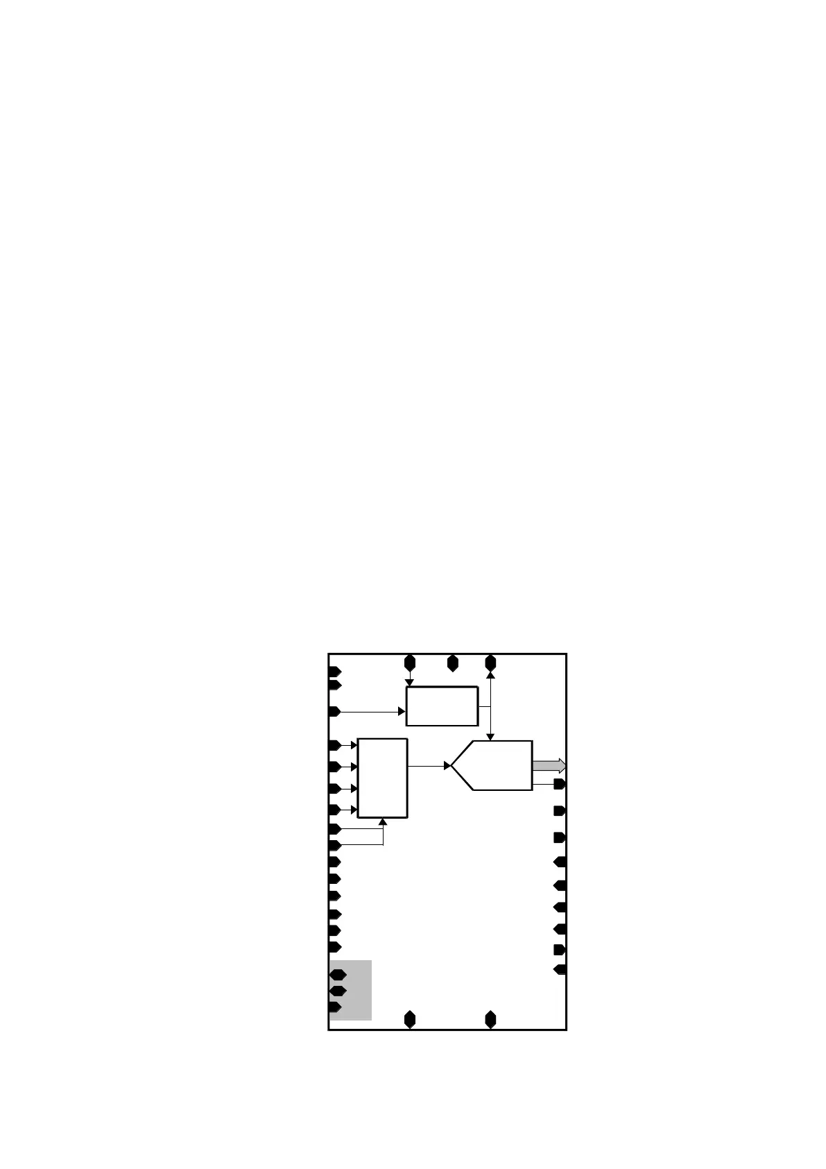
This macro-cell is a power and area optimized
Successive-Approximation ADC, having the
resolution selectable between 12, 10, 8 and 6 bit. It
is instantiated in a CMOS 180nm G process.
To maximize flexibility there are serial and parallel
data outputs, and input pins are provided to apply
an external reference voltage, which defines the full-
scale input range. This reference voltage can be the
analog power supply, for rail-to-rail operation.
An internal voltage regulator is included in order to
improve performance when the digital power supply
is connected to the digital core power supply.
A digital calibration algorithm is implemented to
reduce the offset voltage. Furthermore both
differential and single-ended signals can be
processed.
An analog multiplexer is added to enable selection
from a number of inputs.
This cell is suitable to serve as an auxiliary ADC of
a microprocessor, as a house-keeping converter for
digital applications and broadband wireless
communications.