DWC ADC 12b5M SAR, TSMC180 IP Databook
April 2012 Synopsys, Inc. 19-30
8 Digital Offset Calibration
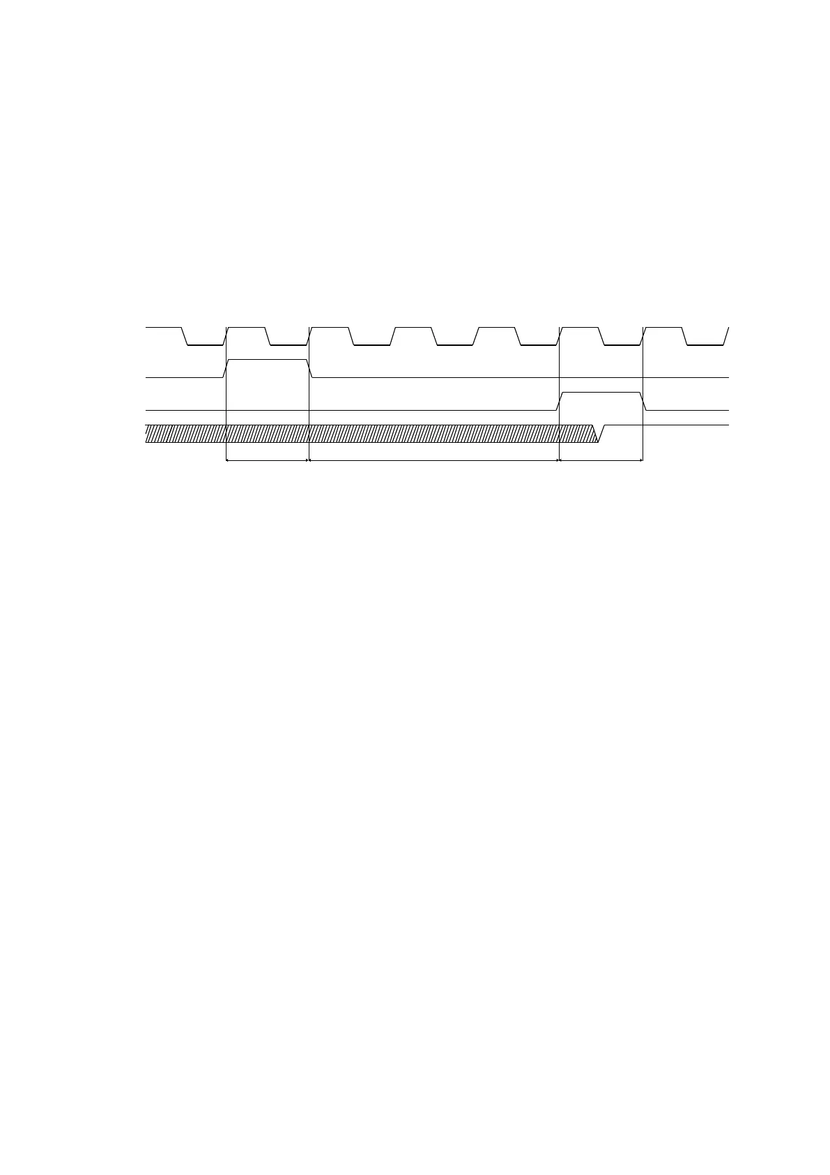
A digital block aids the measurement and correction the offset voltage of the ADC. The
calibration cycle is started as shown in the figure below. First it is necessary to reset the
digital calibration block, placing resetcal at high for, at least, one clock cycle (a clock falling
edge must occur when this signal is high). The startcal signal, whose minimum duration is
also one clock cycle (a clock falling edge must occur when this signal is high), should be
activated 3 clock cycles minimum after the resetcal signal has been deactivated. The calon
is placed at high when the calibration starts and returns to low, when it ends.
Figure 10 - Start of Calibration Cycle
The input of the ADC is reconfigured such that the inputs (after the input selection
multiplexer) are connected internally insuring that a voltage corresponding to the ideal code
„0‟ is sampled. This reconfiguration depends on the ADC input Mode. In this way, before the
calibration cycle, the ADC should be placed in single-ended or differential input mode (by
controlling seldiff signal) for single-ended (seldiff=L) or differential (seldiff=H), respectively.
Part of the input capacitor array is controlled by the successive approximation circuitry
(which is the same used to obtain the output code in normal operation) to measure and
cancel the offset voltage. Every offset voltage measurement/cancellation cycle is performed
using 7 bits (bvos0...bvos6), which allows to correct offset voltages up to +/- 64 LSBs, and
lasts for 8 clock cycles.
To decrease the effect of electrical random noise, the digital block performs an average of
results obtained in 8 consecutive offset measurement cycles: (bvos0...bvos6)
avg
. Afterwards,
in normal operation, the digital block applies (bvos0...bvos6)
avg
to the capacitor array, so that
the offset voltage is removed.
The figure below shows the timing diagram of the full calibration cycle. The result from the 1
st
offset measurement cycle is ignored. A complete calibration cycle lasts 81 clock cycles.
If the startcal signal is still high when calon goes low (end of calibration), a new calibration
cycle is started.
Before and during calibration cycle, soc signal must remain low. After the calibration cycle is
finished (calon goes low), the soc signal can be held at the high logic value, at any time, to
begin a conversion cycle.
resetcal pulse length
1 clk cycle minimum
clk
1 2 3
resetcal
startcal
calon
resetcal-to-startcal time
3 clk cycles minimum
startcal pulse length
1 clk cycle minimum