DWC ADC 12b5M SAR, TSMC180 IP Databook
April 2012 Synopsys, Inc. 26-30
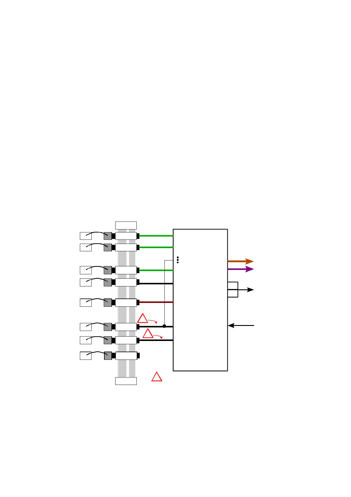
12 Connections to the IO PAD ring
The figures below indicate how the connections between the cell and the IO PAD ring should
be made. The following notation is used:
PVDD1 is a generic 3.3V Power PAD to bias both the IO ring and the core cell.
PGND1 is a generic ground Power PAD to bias both the IO ring and the core cell.
PANA is a generic Analog IO PAD without an internal series ESD resistor.
The connection of dvdd_ldo to an IO PAD should only be considered if the internal voltage
regulator is bypassed (enldo=L) and there is a clean external 1.8V power supply. Otherwise
there is no need to connect this pin to an IO PAD.
Some configuration possibilities will now be illustrated.
The following figure shows the configuration for differential inputs, with external reference
voltage that is independent from supply levels. vrefp and agndref is connected to a pad.
In the case of single ended inputs, the unused negative input should be connected to
agndref.
The connection of agndref and vrefp to the pad, should be made short in order to minimize
the IR drop.
Figure 14 - IO ring case 1 – Separate Analog IO ring when vrefp and agndref applied
externally, vrefp and agndref are connected to a pad, and the inputs are differential.
Analog VDD
Power Cut
PVDD1
PANA
vrefp
vinp18
PGND1
vinn18
vinn0
IO Rings
Power Cut
PANA
PANA
avdd
SAR
ADC
vrefp
vinp18
vinn18
vinn0
agnd
agndref
in case not
used
dvdd
dgnd
Digital Core VDD
Digital Core Ground
All digital
inputs
From Digital
Core
IR droop is critical
b11..0
To Digital Core
eoc
sob
PANA
Analog GND
agndref
dvdd_ldo
dvdd_ldo
......
PVDD1