DWC ADC 12b5M SAR, TSMC180 IP Databook
April 2012 Synopsys, Inc. 18-30
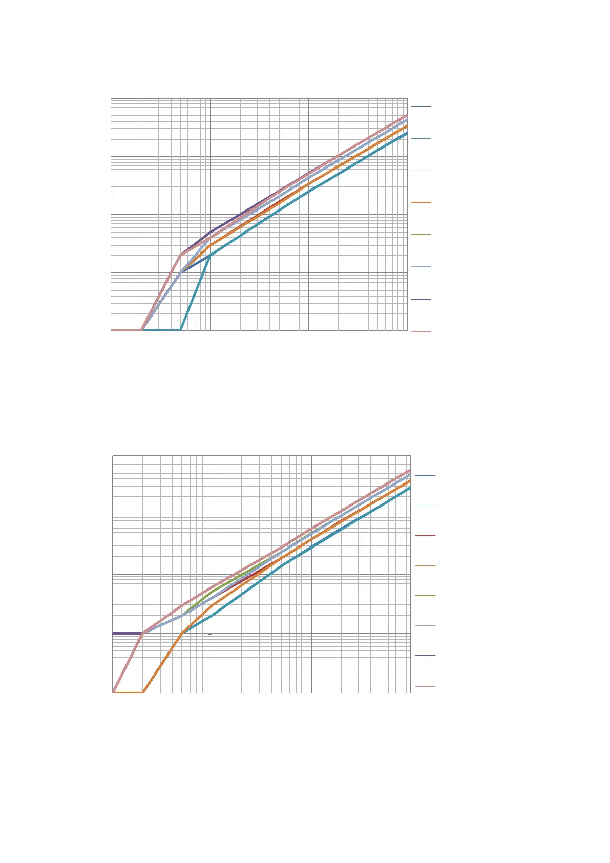
Figure 8 - Additional clock cycles (k) as a function of the signal source output resistance
R
I
(kΩ). The results presented in this graphic were measured under nominal conditions
(typical process corner, avdd = 3.3V, dvdd = 1.8V, Tjunction= 50°C, fclk=70MHz,
vrefp=avdd).
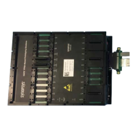
Figure 9 - Additional clock cycles (k) as a function of the signal source output resistance
R
I
(kΩ). The results presented in this graphic were measured under worst case conditions
(slow process corner, avdd = 1.8V, dvdd=1.62V, Tjunction=-40°C, fclk=70MHz, vrefp=avdd).
0
1
10
100
1000
0.1 1.0 10.0 100.0
Additional n' of clock cycles
0
1
10
100
1,000
0.1 1.0 10.0 100.0
Additional n' of clock cycles