DWC ADC 12b5M SAR, TSMC180 IP Databook
April 2012 Synopsys, Inc. 17-30
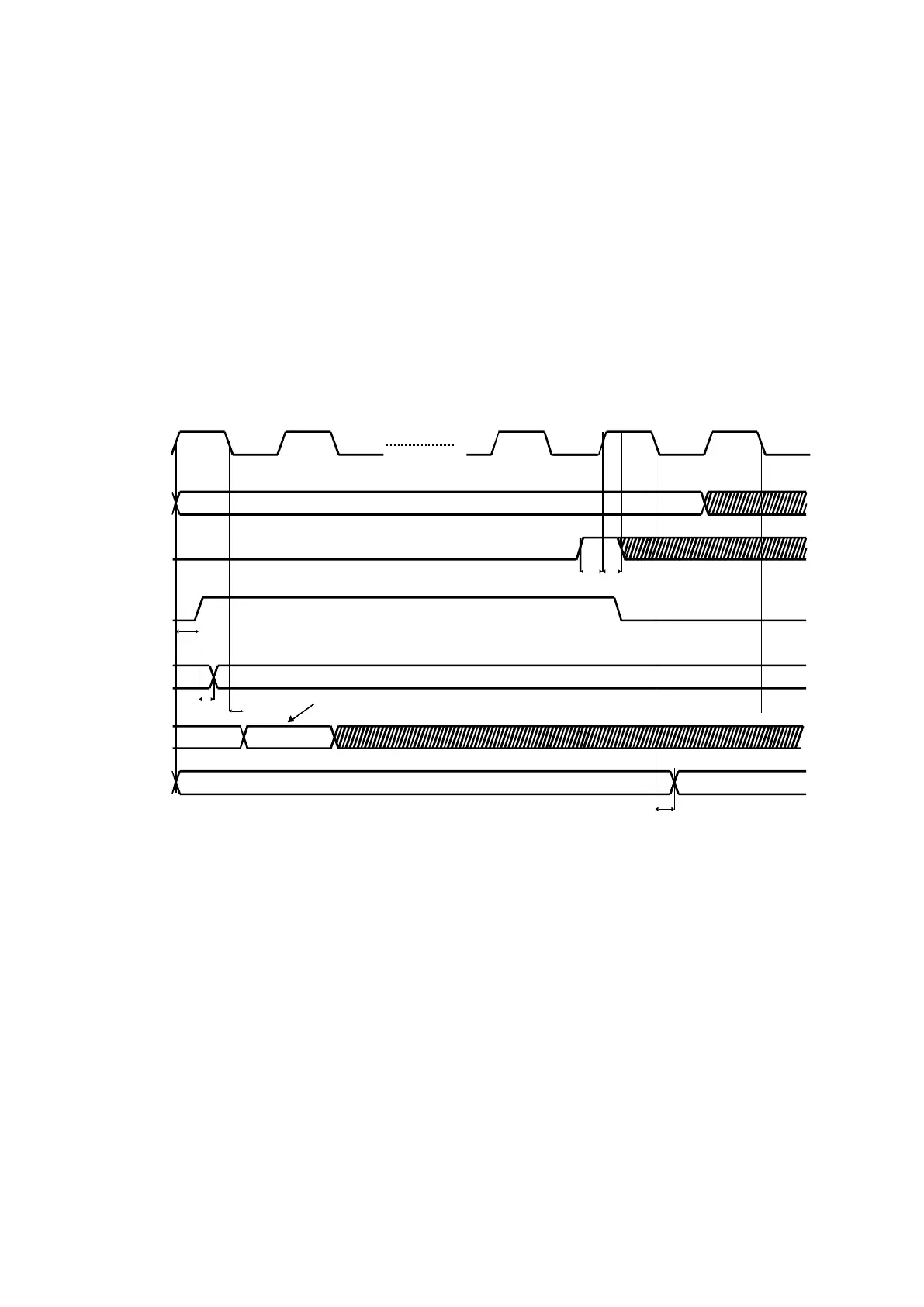
The Figure 7 shows how the sampling time can be increased, to allow the operation with
signal sources having a low driving capability: the soc signal is delayed during the number of
clock cycles necessary to guarantee the accurate input signal sampling. During this period
the input selection bits (sel4..0) must remain unchanged. Note that this operation reduces
the effective sampling rate.
This ADC has two types of inputs: vinp|n5…0 are fast inputs and vinp|n18…6 are slow
inputs. All inputs have the same functionality, but during the sampling period, vinp|n5…0
inputs are faster than vinp|n18…6 inputs.
For both types of inputs, it is possible to achieve the maximum sampling frequency, but
under certain conditions (depending either from the resolution mode (selres) and from the
output impedance of the signal source) the sampling period should be delayed during the
necessary clock cycles to guarantee the sampling precision (Figure 7).
Figure 7 - N: Resolution, that is selectable with selres.
The following graphics indicates the number of wait cycles (k), necessary for a wide range of
R
I
(signal source output resistance) values, for both fast and slow inputs and depending on
the resolution mode (selres).
Please note that these graphics refer to the additional sampling clock cycles. In the
situations where k=0, the sampling period is 1.5 × fclk.
A detailed overview of the sampling time needed for different source impedances and ADC
resolutions in shown in Appendix A table, for the worst case conditions (slow process corner,
avdd = 1.8V, dvdd = 1.62V, Tjunction= -40°C, fclk=70MHz, vrefp=avdd). The sampling time
presented in Appendix A refers to the minimum sampling time to ensure the sampling
precision for each resolution mode.
tsocst tsochld
tdata
Sample Vin(j)
clk
sel4..0
soc
eoc
b11... b0
Internal
S/H
Select Vin(j) channel
Output Data j-1
wait 1 wait k
N+2
1 2
Hold Vin(j)
sob
b
11-N
(sample j-1)
tdatas
teocr
LSB of sample j-1
b
10-N
(sample j-1)