DWC ADC 12b5M SAR, TSMC180 IP Databook
April 2012 Synopsys, Inc. 16-30
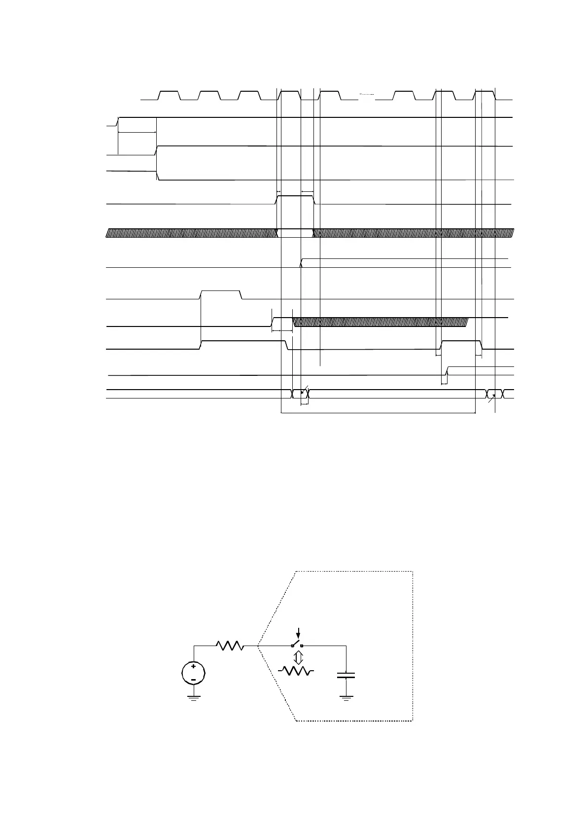
Figure 5 - Startup Sequence from deep power down mode.
The figure below shows the (simplified) equivalent circuit of the S/H input network, where C
S
is the storage capacitor, R
S
is the resistance of the sampling switch and R
I
is the output
impedance of the signal source (v
I
). The Figure 3 shows the situation where the conversion
cycle j+1 starts immediately after conversion cycle n ends. In this case the duration of the
sampling phase is, approximately, 1.5/f
clk
. C
S
must be charged in that phase, and it must be
ensured that the voltage at its terminals becomes sufficiently near v
I
. To guarantee this, R
I
may not take arbitrarily large values.
Figure 6 - Model of the sampling network.
tsocst tsochld
teocr teocf
tdata
tsd
Hold Vin(n)
Sample Vin(n+1)
Sample Vin(n)
soc
eoc
b11... b0
Internal
S/H
reset
Dummy Conversion Cycle
dislvl
bvos6..bvos0
tloadcalsetup tloadcalhold
loadcal
1 2 11 12 1
clk
xx-1
enldo
enadc
...
tup_ldo
bvosi6..bvosi0