DWC ADC 12b5M SAR, TSMC180 IP Databook
April 2012 Synopsys, Inc. 15-30
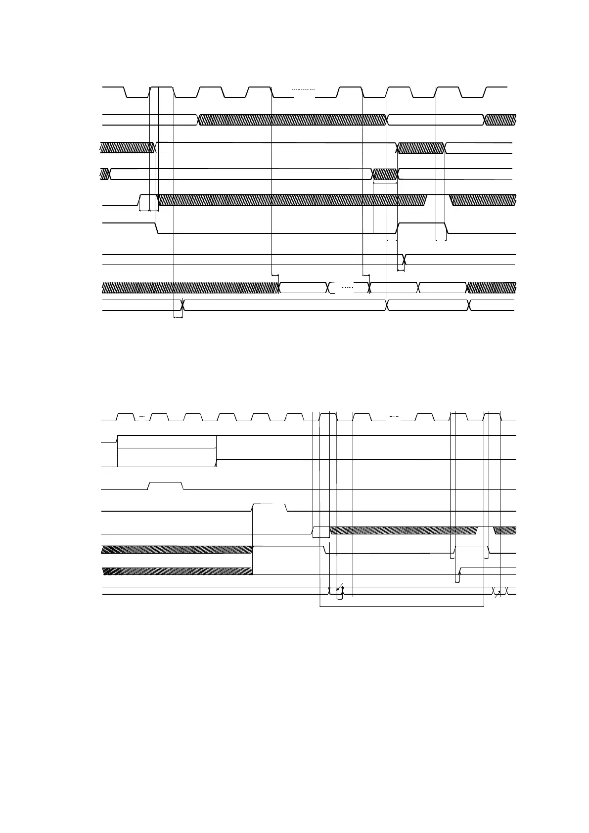
Figure 3 – Normal operation (successive conversions). N: Resolution.
The timing Diagram below shows the startup sequence, in applications where the offset is
not a critical parameter (it is assumed that dislvl is already low). If the offset is critical, then a
calibration cycle should be triggered, as described in section 8. In this timing diagram is
described both the internal regulator and the ADC start-up.
Figure 4 - Startup Sequence from power down mode
The Sample-and-Hold (S/H) starts sampling the input voltage when eoc goes high until tsd
nanosecond after the clock falling edge in the 1
st
cycle. The input selection bits (sel4..0) and
the ADC input mode selection (seldiff) must remain unchanged during this period.
The timing Diagram below shows the start-up sequence from deep power down mode. It
assumes that calibration has been performed in a previous normal operation cycle and that
the calibration value has been stored outside the IP before entering deep power down mode.
If a new calibration cycle is to be run, please refer to the description of the calibration cycle
in section 8.
tsocst tsochld
teocr teocf
tdata
tsd
Hold Vin(j)
Sample Vin(j+1)
Sample Vin(j)
1 2 N+1 N+2 1
clk
sel4..0
soc
eoc
b11... b0
Internal
S/H
x
Select Vin(j) channel Select Vin(j+1) channel
Hold Vin(j+1)
Output Data j
Output Data j-1
b
11sob
b
11-N
tdatas
b
8
b
12-N
tdatas
3
b
10-N
selres Select ADC resolution Select ADC resolution
seldiff Select ADC input mode Select ADC input mode
tclk/2
tsocst tsochld
teocr teocf
tdata
tsd
Hold Vin(n)
Sample Vin(n+1)
Sample Vin(n)
1 2 11 12 1
clk
soc
eoc
b11...0
Internal
S/H
x
resetadc
x-1
enldo
enadc
tup_ldo
resetcal