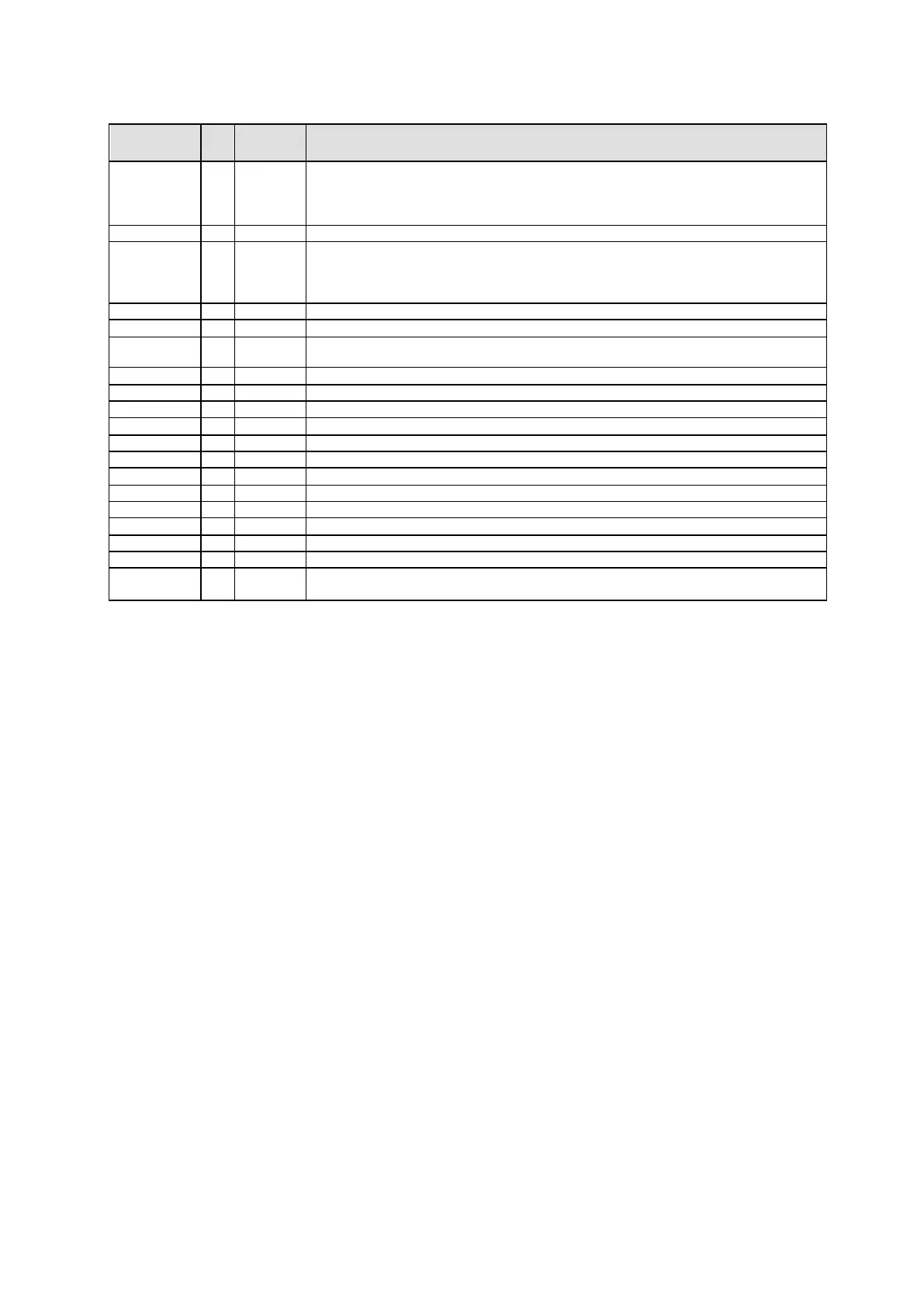
DWC ADC 12b5M SAR, TSMC180 IP Databook
April 2012 Synopsys, Inc. 9-30
Parallel Output Bits. The MSB is b11; the LSB is b0 in 12-bit mode, b2 in 10-bit mode, b4 in
8-bit mode and b6 in 6-bit mode.
Under ADC test mode it is mandatory to have direct access to this signal from chip pinout or
through registers.
Serial Output Bit (starting from the MSB).
End-of-conversion. The rising edge indicates that conversion terminated and output data is
valid.
Under ADC test mode it is mandatory to have direct access to this signal from chip pinout or
through registers.
Outputs of the digital offset calibration block.
Input of the digital offset calibration block
Signal that bypasses the offset calibration block (Active H). In this mode bvos6…0 is set to
1000000.
Signal that loads the offset calibration word into the internal registers (Active H)
Signal that starts the offset calibration cycle (Active H).
Reset of internal registers of the digital offset calibration block (Active H).
Indicates if the ADC is in calibration mode (Active H).
Scan chain clock signal. Used to capture the data and shift the patterns through the chain.
Selects between capture (scanen = L) and shift (scanen = H) modes.
Configures digital offset calibration block to scan test mode (Active H).
Top and Bottom Analog Pow er Supplies (3.3V).
Top and Bottom Digital Pow er Supplies (1.8V).
Internal voltage regulator output (enldo=H). With enldo=L (internal voltage regulator bypass)
the power signal must be supplied externally(1.8V).