58
paGe HeadClOCK and synCHrOnIzaTIOn In sysTem 6000
%DQGZLGWK $IWHUGHYLFH $IWHUGHYLFH $IWHUGHYLFH $IWHUGHYLFH
50 to 100 kHz 1.0 ns peak 2.2 ns peak 2.5 ns peak 1.1 ns peak
700 to 100 kHz 0.9 ns peak 1.6 ns peak 1.9 ns peak 0.9 ns peak
1200 to 100 kHz 0.9 ns peak 1.5 ns peak 1.7 ns peak 0.9 ns peak
How to detect interface jitter.
The typical way to investigate interface jitter is by
measuring the clock variations directly on the digital signal.
There are devices made specifically for interface testing.
7KHZD\WKH\XVXDOO\ZRUNLVE\DSSO\LQJD3//FLUFXLWOLNH
the ones used for jitter rejection (see The clock design on
System 6000) and then measure the amount that has been
VWRSSHGE\WKH3//
This circuit will act like a low pas filter towards the jitter
variations and therefore it is the high frequencies that
DUHVWRSSHGE\WKH3//7KLVZD\\RXZLOOPHDVXUHWKH
jitter noise with a band limited filter that typically will have
settings like 50 to 100 kHz, 700 to 100 kHz and 1200 to
100kHz.
%\DSSO\LQJGLIIHUHQWILOWHUVDQGWKHUHIRUHJHWWLQJGLIIHUHQW
results you will have an idea of what jitter amount your
system is operating at and what jitter frequencies that
might be the potential problem.
Examples of interface jitter amounts
A test setup was made with 4 different devices connected
XVLQJ$(6(%86KRUWLPSHGDQFHPDWFKHGFDEOHVZHUH
used so there was only an insignificant amount of jitter
coming from this potential source.
Figure 2. Test setup for interface jitter measurement.
Devices 1 to 3 are conventional designs with no jitter
rejection below 10 kHz.
Device 4 is System 6000 (with jitter rejection).
Table 1 Interface jitter measurements.
In Table 1 the results from the interface jitter
measurements are shown. After device 1 the results
reflect only intrinsic jitter of this machine. Notice the slight
increase at 50Hz, which is common. After device 2 the
jitter amount has increased which in this case was due to
intrinsic jitter in device 2. The same thing was the case
after device 3. After System 6000 (device 4) jitter level has
dropped due to the jitter rejection in the system.
There is still an increased level at 50Hz where the System
6000 jitter rejection filter has it’s corner frequency and this
is why the jitter at 50Hz isn’t as reduced as the level above
50Hz.
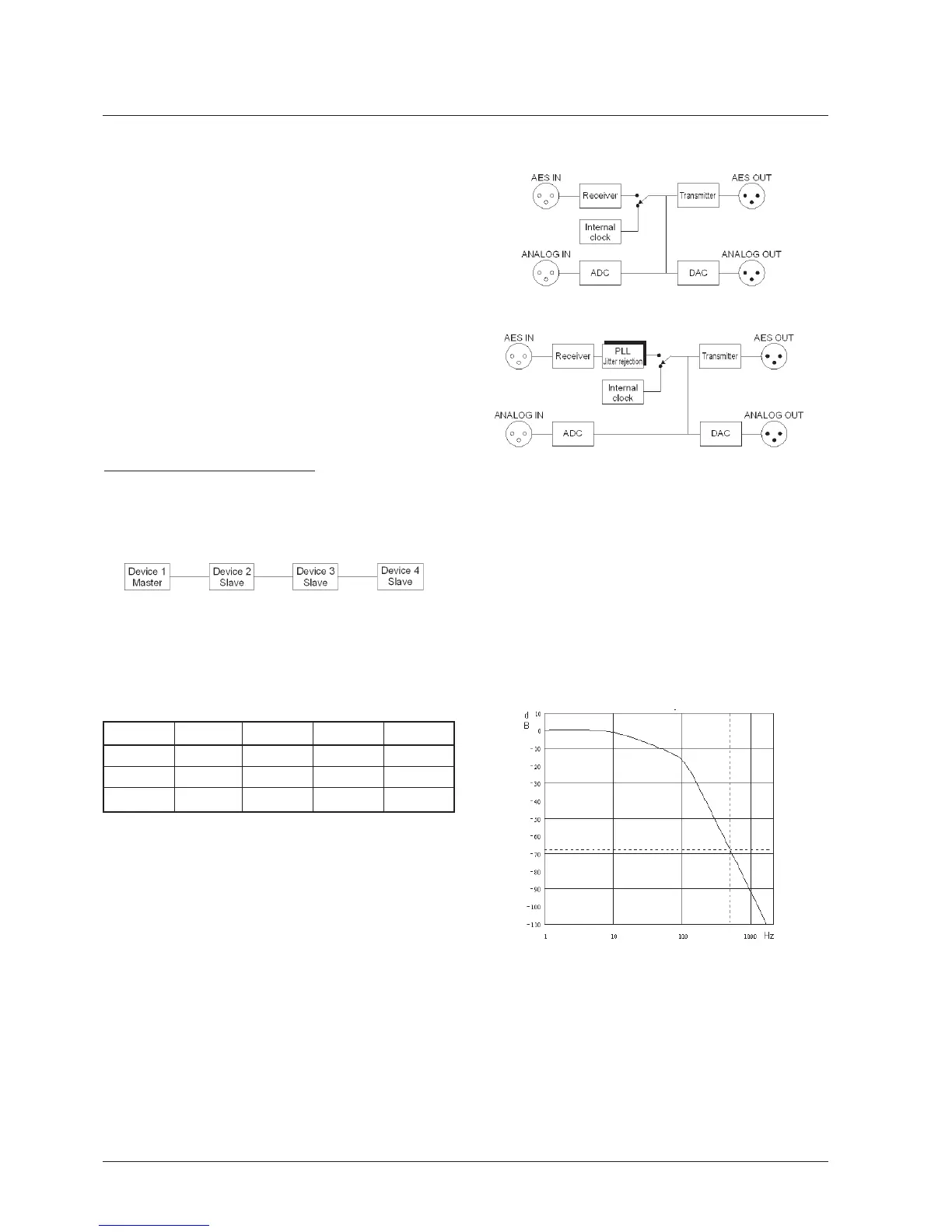
The clock design on System 6000
Figure 3 Clock circuit in a conventional design and in
System 6000
Jitter rejection
7KHVHFUHWLVWKH3//WKDWLVXVHGWRUHPRYHMLWWHUWKDW
might appear on the digital input and in a conventional
design is transferred nearly directly to the converters. The
3//DFWVDVDORZSDVVILOWHUDQGZLOOUHGXFHMLWWHUQRLVHRI
higher frequencies than the corner frequency of the filter.
On System 6000 the corner frequency is as low as 50 Hz
and at 1.4 kHz the noise will be reduced by at least 100
G%)LJXUHVKRZVG%DW+]ZKLFKFRUUHVSRQGVWR
filter suggestions, made from research in the last year’s [1].
Figure 4 Jitter rejection filter (4’Th order filter)
It is very difficult to design a low pass filter with a steep
slope without gain in the pass band. This type of gain can
contribute to jitter accumulation in a chain of devices. The
6\VWHPJDLQVDVOLWWOHDVG%DW+]
 Loading...