Section IV – Diagrams
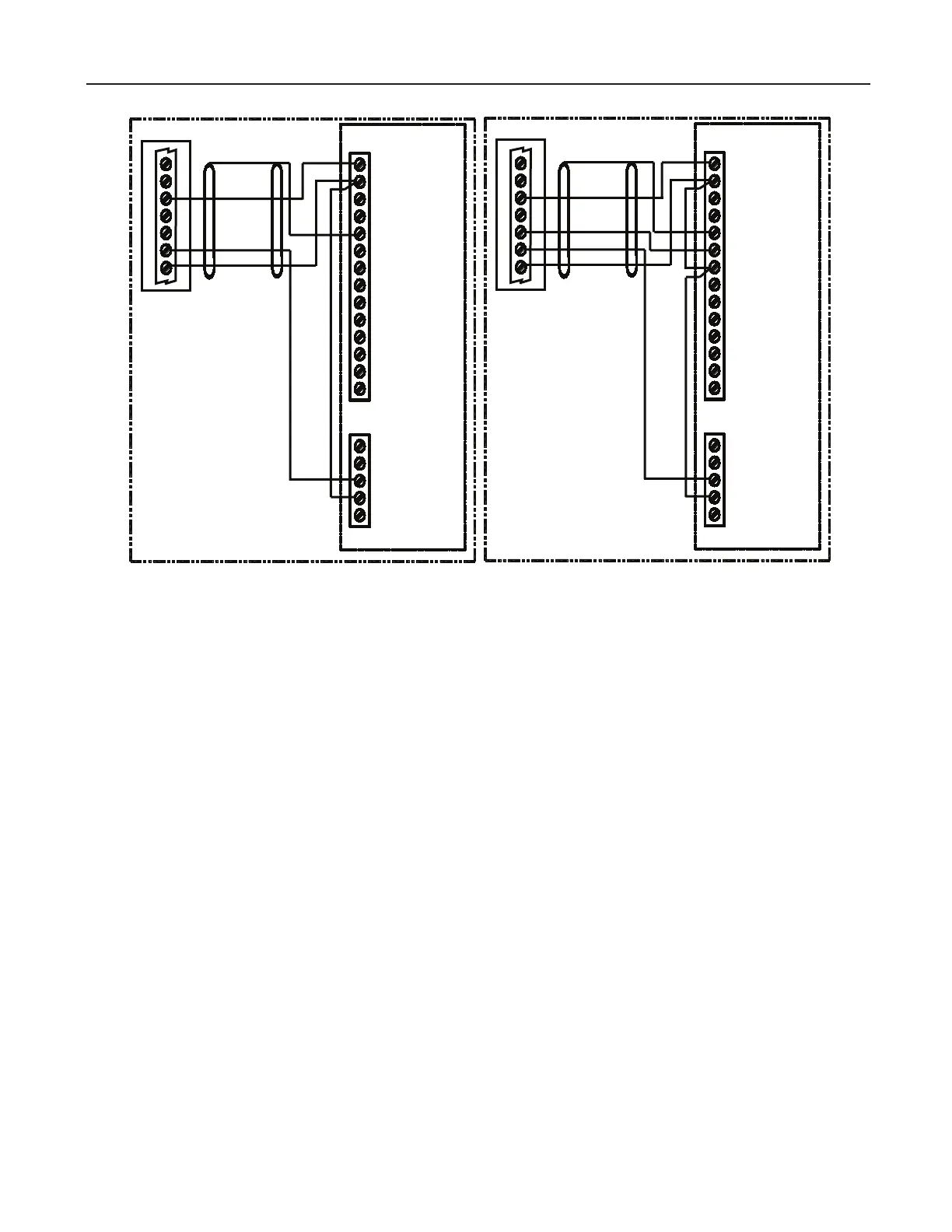
Figure 10. Wiring Diagram, Universal Pulse Transmitter (UPT)
UPT Terminal Connections:
1. Electronics Ground
2. Input Power (12-24 Vdc)
4. Channel “B” Inverse Output
5. Channel “A” Output
6. Channel “A” Inverse Output
7. Shield
10. Not Used
Note: Pulse Inputs
• If EPLD (U24 chip) is Rev. 0, dual pulse will not function under 25 Hz. Only single pulse will count from 25 Hz
down to 3 Hz. Above 25 Hz, dual pulse will function as normal.
• If EPLD (U24 chip) is Rev. 1 or higher, dual pulse will function from 3 Hz and higher.
• Pulse doubling will not function for input pulses below 25 Hz.
14
13
12
11
10
9
8
7
6
5 Shield
4
3
2 A-
1 A+
CN5
5
4 Gnd
3 +12Vdc
2
1
CN6
UPT
MNET Board
UPT, Single Pulse
4
5
6
7
3
2
1
14
13
12
11
10
9
8
7 B-
6 B+
5 Shield
4
3
2 A-
1 A+
CN5
5
4 Gnd
3 +12Vdc
2
1
CN6
UPT
MNET Board
UPT, Dual Pulse
4
5
6
7
3
2
1