Theory of Operation—2465B/2467B Service
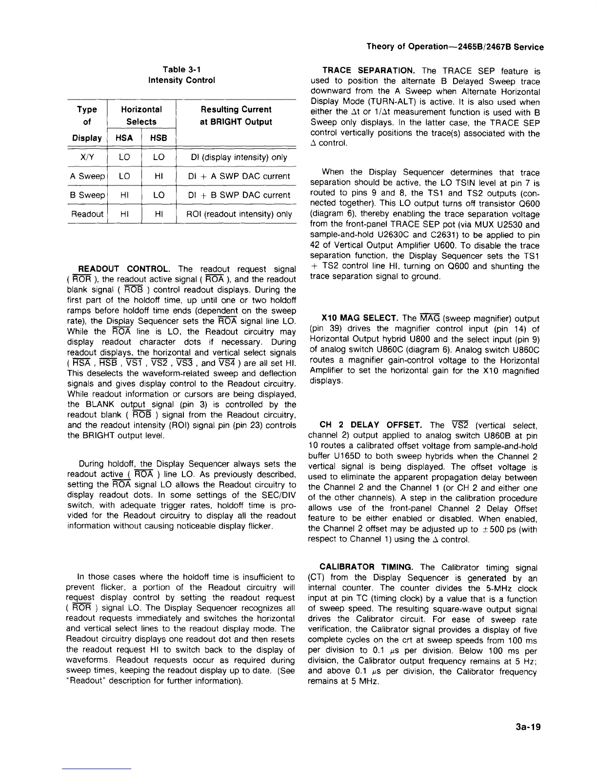
Table 3-1
Intensity Control
Type
of
Display
X/Y
A Sweep
B Sweep
Readout
Horizontal
Selects
HSA
LO
LO
HI
HI
HSB
LO
HI
LO
HI
Resulting Current
at BRIGHT Output
Dl (display intensity) only
Dl + A SWP DAC current
Dl + B SWP DAC current
ROI (readout intensity) only
READOUT CONTROL. The readout request signal
( ROR ), the readout active signal ( ROA ), and the readout
blank signal ( ROB ) control readout displays. During the
first part of the holdoff time, up until one or two holdoff
ramps before holdoff time ends (dependent on the sweep
rate),
the Display Sequencer sets the ROA signal line LO.
While the ROA line is LO, the Readout circuitry may
display readout character dots if necessary. During
readout displays, the horizontal and vertical select signals
( HSA , HSB , VST , VS2 , VS3 , and VS4 ) are all set HI.
This deselects the waveform-related sweep and deflection
signals and gives display control to the Readout circuitry.
While readout information or cursors are being displayed,
the BLANK output signal (pin 3) is controlled by the
readout blank ( ROB ) signal from the Readout circuitry,
and the readout intensity (ROI) signal pin (pin 23) controls
the BRIGHT output level.
During holdoff, the Display Sequencer always sets the
readout active ( ROA ) line LO. As previously described,
setting the ROA signal LO allows the Readout circuitry to
display readout dots. In some settings of the SEC/DIV
switch,
with adequate trigger rates, holdoff time is pro-
vided for the Readout circuitry to display all the readout
information without causing noticeable display flicker.
In those cases where the holdoff time is insufficient to
prevent flicker, a portion of the Readout circuitry will
request display control by setting the readout request
( ROR ) signal LO. The Display Sequencer recognizes all
readout requests immediately and switches the horizontal
and vertical select lines to the readout display mode. The
Readout circuitry displays one readout dot and then resets
the readout request HI to switch back to the display of
waveforms. Readout requests occur as required during
sweep times, keeping the readout display up to date. (See
"Readout" description for further information).
TRACE SEPARATION. The TRACE SEP feature is
used to position the alternate B Delayed Sweep trace
downward from the A Sweep when Alternate Horizontal
Display Mode (TURN-ALT) is active. It is also used when
either the At or 1/At measurement function is used with B
Sweep only displays. In the latter case, the TRACE SEP
control vertically positions the trace(s) associated with the
A control.
When the Display Sequencer determines that trace
separation should be active, the LO TSIN level at pin 7 is
routed to pins 9 and 8, the TS1 and TS2 outputs
(con-
nected together). This LO output turns off transistor Q600
(diagram 6), thereby enabling the trace separation voltage
from the front-panel TRACE SEP pot (via MUX U2530 and
sample-and-hold U2630C and C2631) to be applied to pin
42 of Vertical Output Amplifier U600. To disable the trace
separation function, the Display Sequencer sets the TS1
+ TS2 control line HI, turning on Q600 and shunting the
trace separation signal to ground.
X10 MAG SELECT. The MAG (sweep magnifier) output
(pin 39) drives the magnifier control input (pin 14) of
Horizontal Output hybrid U800 and the select input (pin 9)
of analog switch U860C (diagram 6). Analog switch U860C
routes a magnifier gain-control voltage to the Horizontal
Amplifier to set the horizontal gain for the X10 magnified
displays.
CH 2 DELAY OFFSET. The VS2 (vertical select,
channel 2) output applied to analog switch U860B at pin
10 routes a calibrated offset voltage from sample-and-hold
buffer U165D to both sweep hybrids when the Channel 2
vertical signal is being displayed. The offset voltage is
used to eliminate the apparent propagation delay between
the Channel 2 and the Channel 1 (or CH 2 and either one
of the other channels). A step in the calibration procedure
allows use of the front-panel Channel 2 Delay Offset
feature to be either enabled or disabled. When enabled,
the Channel 2 offset may be adjusted up to ± 500 ps (with
respect to Channel 1) using the A control.
CALIBRATOR TIMING. The Calibrator timing signal
(CT) from the Display Sequencer is generated by an
internal counter. The counter divides the 5-MHz clock
input at pin TC (timing clock) by a value that is a function
of sweep speed. The resulting square-wave output signal
drives the Calibrator circuit. For ease of sweep rate
verification, the Calibrator signal provides a display of five
complete cycles on the crt at sweep speeds from 100 ms
per division to 0.1 ^s per division. Below 100 ms per
division,
the Calibrator output frequency remains at 5 Hz;
and above 0.1 ^s per division, the Calibrator frequency
remains at 5 MHz.
3a-19

 Loading...


