Theory of Operation—2465B/2467B Service
Triggers
The A/B Trigger hybrid (U500) and associated circuitry
select the triggering signal source for each horizontal
sweep as directed by the Display Sequencer. When the
proper triggering criteria to initiate a sweep are detected, a
triggering gate signal is produced to start the selected
sweep.
Control data from the processor defining trigger mode,
coupling,
and slope parameters for each trigger is clocked
into two storage registers internal to U500 by the A TRIG
CLK signal on pin 23 ( CCA ) and the B TRIG CLK signal
on pin 47 ( CCB ). The Display Sequencer selects the A
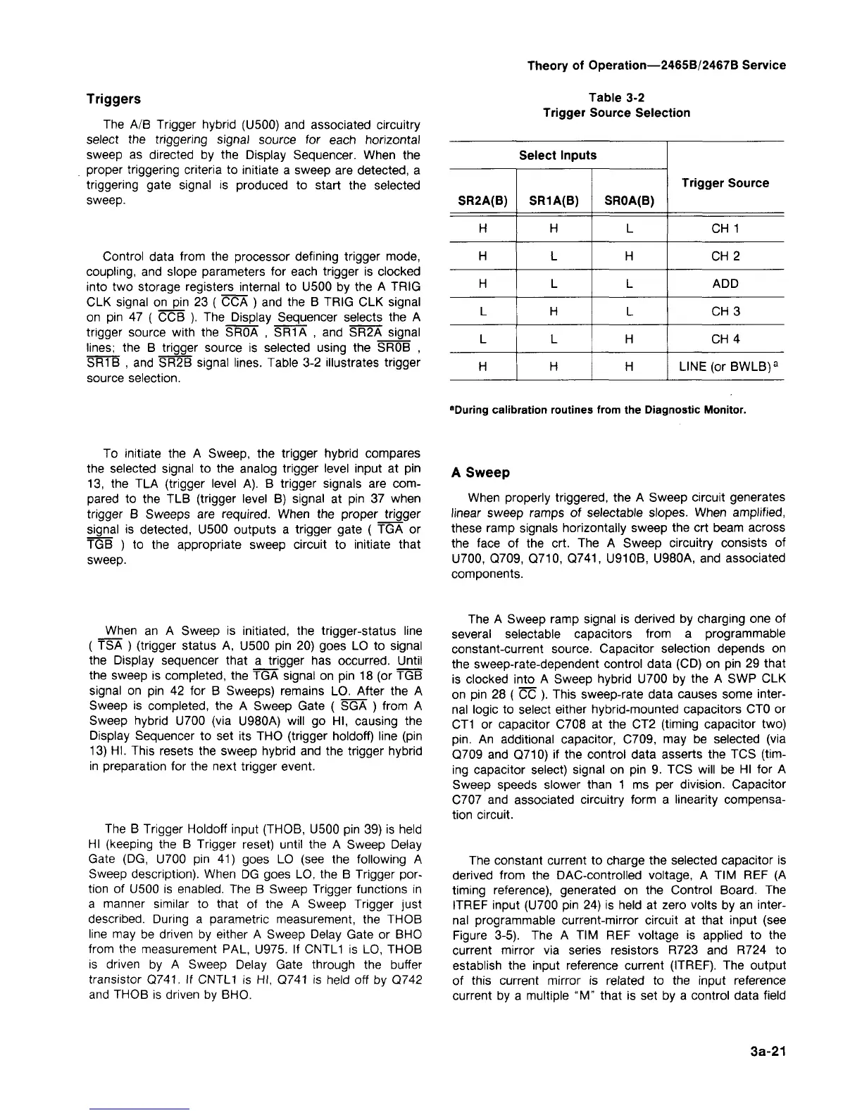
trigger source with the SROA , SR1A , and SR2A signal
lines;
the B trigger source is selected using the SROB ,
SR1B , and SR2B signal lines. Table 3-2 illustrates trigger
source selection.
To initiate the A Sweep, the trigger hybrid compares
the selected signal to the analog trigger level input at pin
13,
the TLA (trigger level A). B trigger signals are com-
pared to the TLB (trigger level B) signal at pin 37 when
trigger B Sweeps are required. When the proper trigger
signal is detected, U500 outputs a trigger gate ( TGA or
TGB ) to the appropriate sweep circuit to initiate that
sweep.
When an A Sweep is initiated, the trigger-status line
( TSA ) (trigger status A, U500 pin 20) goes LO to signal
the Display sequencer that a trigger has occurred. Until
the sweep is completed, the TGA signal on pin 18 (or TGB
signal on pin 42 for B Sweeps) remains LO. After the A
Sweep is completed, the A Sweep Gate ( SGA ) from A
Sweep hybrid U700 (via U980A) will go HI, causing the
Display Sequencer to set its THO (trigger holdoff) line (pin
13) HI. This resets the sweep hybrid and the trigger hybrid
in preparation for the next trigger event.
The B Trigger Holdoff input (THOB, U500 pin 39) is held
HI (keeping the B Trigger reset) until the A Sweep Delay
Gate (DG, U700 pin 41) goes LO (see the following A
Sweep description). When DG goes LO, the B Trigger por-
tion of U500 is enabled. The B Sweep Trigger functions in
a manner similar to that of the A Sweep Trigger just
described.
During a parametric measurement, the THOB
line may be driven by either A Sweep Delay Gate or BHO
from the measurement PAL, U975. If CNTL1 is LO, THOB
is driven by A Sweep Delay Gate through the buffer
transistor Q741. If CNTL1 is HI, Q741 is held off by Q742
and THOB is driven by BHO.
Table 3-2
Trigger Source Selection
Select Inputs
SR2A(B)
H
H
H
L
L
H
SR1A(B)
H
L
L
H
L
H
SROA(B)
L
H
L
L
H
H
Trigger Source
CH 1
CH 2
ADD
CH3
CH4
LINE (or BWLB)
a
"During calibration routines from the Diagnostic Monitor.
A Sweep
When properly triggered, the A Sweep circuit generates
linear sweep ramps of selectable slopes. When amplified,
these ramp signals horizontally sweep the crt beam across
the face of the crt. The A Sweep circuitry consists of
U700,
Q709, Q710, Q741, U910B, U980A, and associated
components.
The A Sweep ramp signal is derived by charging one of
several selectable capacitors from a programmable
constant-current source. Capacitor selection depends on
the sweep-rate-dependent control data (CD) on pin 29 that
is clocked into_ A Sweep hybrid U700 by the A SWP CLK
on pin 28 ( CC ). This sweep-rate data causes some inter-
nal logic to select either hybrid-mounted capacitors CTO or
CT1 or capacitor C708 at the CT2 (timing capacitor two)
pin.
An additional capacitor, C709, may be selected (via
Q709 and Q710) if the control data asserts the TCS
(tim-
ing capacitor select) signal on pin 9. TCS will be HI for A
Sweep speeds slower than 1 ms per division. Capacitor
C707 and associated circuitry form a linearity compensa-
tion circuit.
The constant current to charge the selected capacitor is
derived from the DAC-controlled voltage, A TIM REF (A
timing reference), generated on the Control Board. The
ITREF input (U700 pin 24) is held at zero volts by an inter-
nal programmable current-mirror circuit at that input (see
Figure 3-5). The A TIM REF voltage is applied to the
current mirror via series resistors R723 and R724 to
establish the input reference current (ITREF). The output
of this current mirror is related to the input reference
current by a multiple "M" that is set by a control data field
3a-21