Theory of Operation—465B Service
CHANNEL
1 DISPLAY ONLY.
When the CH
1
VERT
MODE push
button is pressed,
a HI Is
applied to the
A)
Input of
U1605.
The
A4. A?,
and
At
Inputs will
be LO and the
A?
input
(controlled by
the
X-Y
position
of the A TIME/DIV
switch)
will be HI.
This combination
of inputs
is decoded
to
switch transistor
Q1619 on. which
turns
on
the
Channel
1 Diode
Gate. The
O, output of
U1605 will be
LO.
the
0
2
and
O3 outputs will
be HI. The
0< output, which controls
the CHOP
oscillator,
will be low.
A LO will disable
the
CHOP
clock and
U1705 will remain
in a state
that allows
the Diode
Gates
to pass only the Channel
1 input signal
to
the Delay
Line Driver.
With Channel
1 only selected,
the
Qo
output of
U1705
will
be LO. The LO will turn
on transistor Q1619 and
the
junction
of CR1447 and CR1443 will
be returned
to
the
+5-volt
supply through R1625 andQl619.
This raises the
junction
voltage
to
reverse
bias CR1447 and CR1443.
Then CR1445 and CR1441
are forward biased and
the
Channel
1 input
signal passes through
CR1441 and
CR1445 to the Delay-Line
Driver
CR1432
and CR1434 in the Trigger
View Diode Gate
and CR1547
and CR1543 in the Channel
2
Vertical Signal
Diode Gate remain forward
biased through the pull-down
resistors
to the
—8
volt power supply.
Trigger View signals
and the Channel
2 input signals are
shunted to the 8 volt
supply and
are blocked from
the Delay Line Driver
because
CR1438 and CR1436 in
the Trigger View Diode
Gate and
CR1545 and CR1541
in the Channel
2
Vertical
Signal
Diode Gate are
reverse biased
CHANNEL
2
DISPLAY
ONLY. When
CH 2 VERT MODE
is selected, 01719
turns on; Q1619 and
Q1617 remain off.
The center diodes
of the Channel 1 Diode
Gate and the
center diodes
of the Trigger
View Diode Gate are forward
biased, and the
center diodes of the Channel
2 Diode Gate
are reverse
biased. Trigger
view and Channel 1 signals are
blocked
from the Delay
Line Driver, and the Channel
2
input
signal is connected
to the Delay Line Driver.
and
the Q
0
and
Qi
outputs will
be HI. This will cause both
Channel 1 and Channel
2 Diode Gates
to be on.
With
Qo
and
Q,
HI.
U1805D
will
be enabled to turn on Q1636.
The
junction of R1532
and
R1534
will have
-8
volts
applied to
provide
sufficient additional current to
keep both Diode
Gates turned on without altering
the dc levels associated
with
the Delay Line Driver. By selecting
additional VERT
MODEs, it is possible
to view the Channel
1
input,
the
Channel
2 input, the
A External
Trigger
input, and
ADD
MODE on the ert during
one display cycle on four
separate
traces.
X-Y MODE. When the
A
TIME/DIV
switch is set to X-Y, a
LO is applied to pin
15
of
U1
605.
The ROM is programmed
to
produce outputs that turn
on Channel 2 switching
transistor
Q1719 and disable the CHOP clock.
This action
causes the Channel 2 input to
be
connected
to the Delay
Line Driver for the Y-axis
signal. It is not necessary to
select
Channel
2
VERT
MODE,
since
the ROM will not
respond
to any
other
input while the
X-Y
mode is selected
Chop
Clock and Alternate Logic
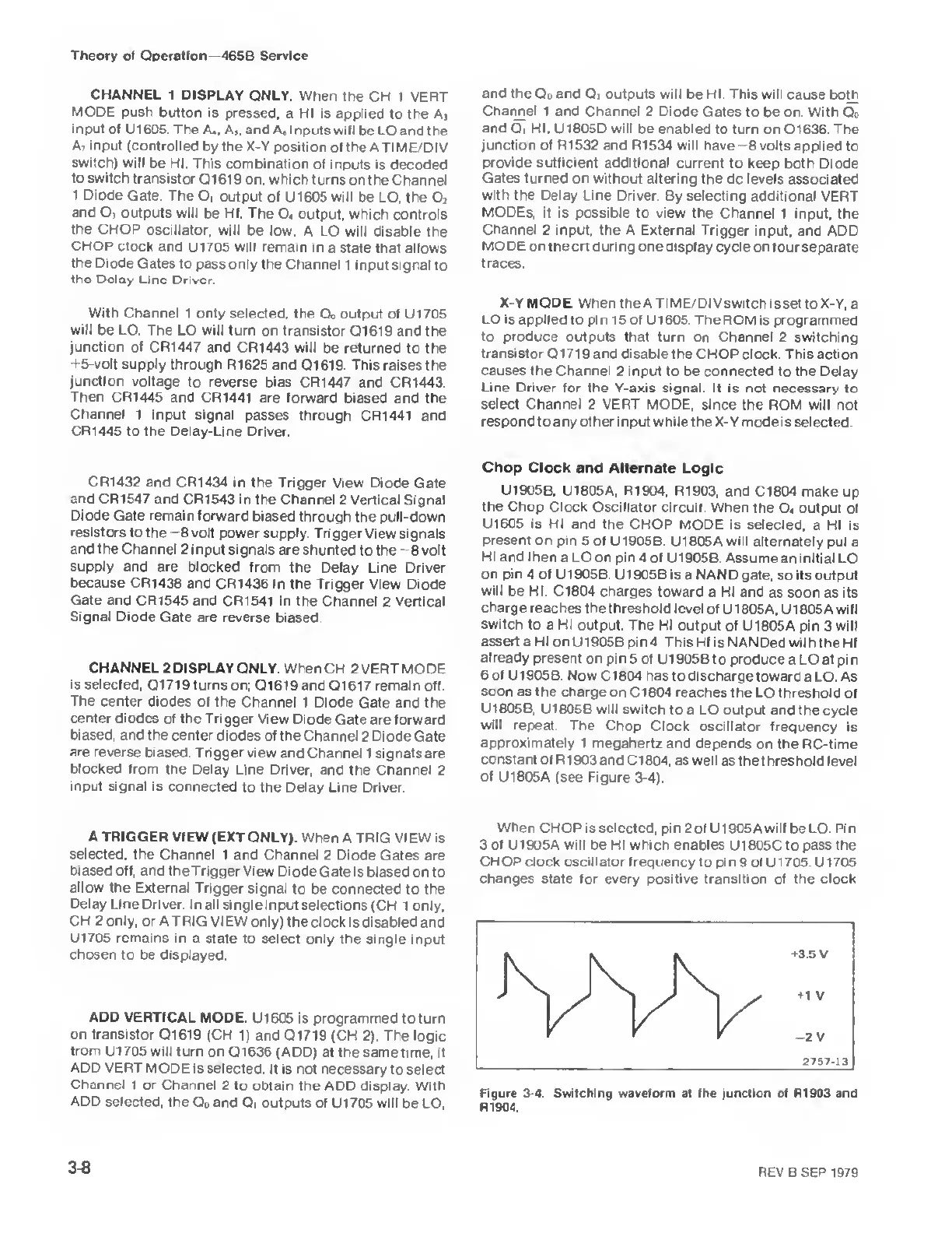
U1905B, U1805A, R1904, R1903,
and Cl 804 make
up
the Chop
Clock Oscillator circuit.
When the
0«
output
of
U1605
is
HI
and the CHOP MODE is
selected, a HI is
present
on pm 5 of
U1905B U1805A will alternately
put a
HI
and then a LO on pin 4
of U1905B
Assume an initial LO
on pin 4 of
U1905B U1905B is a NAND
gate, so its output
will
be HI. Cl 804
charges toward
a
HI
and as soon as its
charge
reaches the threshold
level of
U1805A, U1805A will
switch to
a
HI
output The HI
output of U1805A pin
3
will
assert
a HI on U1905Bpin4 This HI isNANDed
with
the HI
already
present
on pin 5 of
U1905B to produce a LO at pin
6 of U1905B. Now
C1804 has to discharge
toward a LO. As
soon
as the charge
on Cl 804 reaches the
LO threshold of
U1805B, U1805B will
switch to a LO output
and the cycle
will
repeat The
Chop Clock oscillator
frequency
is
approximately
1
megahertz
and
depends on the RC-time
constant
of Ri 903 and
Cl 804, as well as the threshold
level
of
U 1805
A
(see Figure 3-4).
A TRIGGER VIEW
(EXT ONLY). When
A TRIG VIEW is
selected, the
Channel 1 and Channel
2 Diode Gates are
biased off, and
theTrigger View Diode
Gateisbiased on to
allow the External
Trigger signal
to be connected to the
Delay Line Driver.
In all single input
selections (CH 1 only,
CH 2 only, or
A
TRIG
VIEW only) the clock
is
disabled
and
U1705
remains
in a state to select
only the single input
chosen to
be displayed.
ADD
VERTICAL
MODE. U1605 is programmed
to
turn
on
transistor
Q1619 (CH
1)
and
Q1719
(CH
2).
The
logic
from U1705 will turn
on Q1636 (ADD)
at the
same
time, if
ADD
VERT MODE is
selected. It
is
not necessary
to select
Channel 1 or Channel
2 to obtain the ADD
display. With
ADD selected, the
Q
0
and
Qi
outputs
of U1705 will be LO,
When CHOP
is
selected, pin
2of U1905A will beLO. Pin
3 of U1905A will
be
HI which enables
U1805Cto pass the
CHOP clock oscillator
frequency to
pin
9 of
U
1705 U 1705
changes state for every positive transition
of
the clock
Figure 3-4. Switching waveform
at the junction of R1903 and
R1904.
38
REV
B
SEP
1979