465B
Service
LIST
OF
ILLUSTRATIONS
(cont)
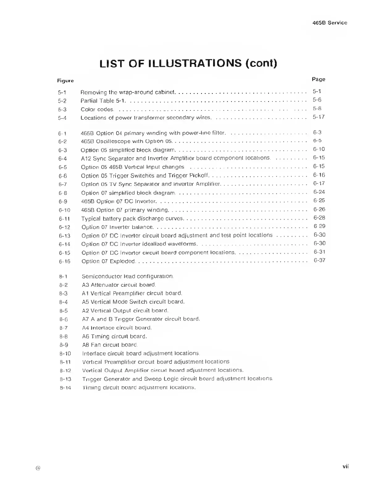
Figure
Pa
9
e
5-1
Removing
the wrap-around
cabinet
5-1
5-2 Partial Table
5-1
5-6
5-3 Color codes
5-8
5-
4
Locations of power
transformer secondary wires
5-17
6-
1
465B Option
04
primary
winding with
power-line filter
6-3
6-2
465B Oscilloscope with
Option
05
6-5
6-3
Option 05
simplified block diagram
6-10
6-4
A12 Sync Separator and
Inverter Amplifier
board component locations
6-15
6-5
Option 05
465B Vertical
Input
changes
6-15
6-6
Option 05 Trigger
Switches and
Trigger Pickoff
6-16
6-7 Option
05 TV
Sync Separator
and Inverter Amplifier
6-17
6-8
Option 07 simplified
block diagram
6-24
6-9
465B
Option 07 DC Inverter
6-25
6-10
465B Option 07 primary
winding
6-26
6-11
Typical
battery pack discharge curves
6-28
6-12
Option 07
Inverter balance
6
29
6-13 Option 07 DC
Inverter circuit board
adjustment and test point
locations
6-30
6-14 Option 07
DC
Inverter idealized
waveforms
6-30
6-15 Option 07
DC
Inverter circuit board
component locations
6-31
6-16
Option 07 Exploded
6-37
8-1
Semiconductor lead
configuration
8-2
A3 Attenuator circuit board
8-3
A1 Vertical Preamplifier
circuit board
8-4
A5 Vertical Mode
Switch circuit board.
8-5
A2
Vertical Output circuit board-
8-6
A7 A and B
Trigger Generator circuit board
8 7 A4 Interface
circuit board.
8-8
A6 Timing circuit board.
8-9
A8 Fan circuit board.
8-10 Interface circuit board adjustment
locations
8-11 Vertical Preamplifier
circuit board adjustment locations
8-12 Vertical Output Amplifier circuit hoard
adjustment locations.
8-13
Trigger Generator
and Sweep Logic circuit
board
adjustment locations
8-14 Timing circuit board adjustment
locations.