ME910C1 mPCIe HW Design Guide
1VV0301642 Rev. 2 Page 22 of 56 2022-01-14
6. DIGITAL SECTION
Logic Levels
All digital signals are powered from the internal module’s V
IO
power bank, V
IO
=1.8V.
All control signals are powered from the external 3V3_AUX power bank, 3V3_AUX=3.3V.
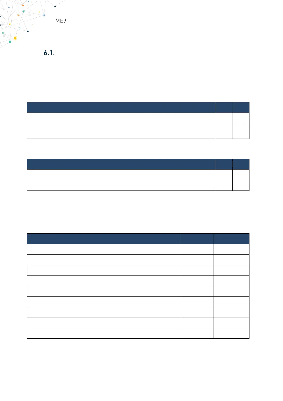
ABSOLUTE MAXIMUM RATINGS:
Table 10 Absolute Maximum Rating digital signals (CMOS 1.8V)
Table 11 Absolute Maximum Rating for control signal
OPERATING RANGE DIGITAL SIGNALS (CMOS 1.8V):
1.2V 1.85V
0V 0.6V
1.4V 1.8V
10kΩ 390kΩ
10kΩ 390kΩ
2mA 3mA
Table 12 Operating range digital signals (CMOS 1.8V)
Input High Voltage on digital signals (CMOS 1.8) with respect to ground when 3V3_AUX is supplied
-0.3V 2.1V
Input High Voltage on digital signals (CMOS 1.8) with respect to ground when 3V3_AUX is not
supplied
-0.3V 0.3V
Input Voltage on control signals with respect to ground when 3V3_AUX is supplied
-0.3V 5V
Input Voltage on control signals with respect to ground when 3V3_AUX is not supplied
-0.3V 0.3V