March 2009 SNAU028A 7
Follow the step-by-step instructions under the “HelpBar” mini-tab (left hand side of the GUI) to
configure the LMP90100 for this example. These step-by-step instructions are discussed in
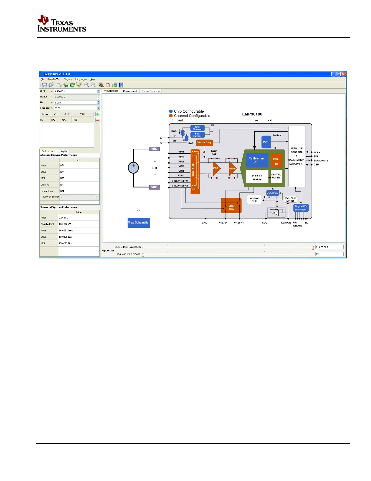
details below, and the recommended configuration should look similar to the figure below.
Figure 5 - Recommended LMP90100 Configuration for a DC Reading
1. Step 1: Select a Sensor - select “DC” “DC” since the input source is not a sensor.
2. Step 2: Configure Inputs – click on the “INPUT MUX” block to set “VINP = 000: VIN2”
and “VINN = 001: VIN3”. Since VIN0 = (3/4) VREF1 and VIN1 = (1/4) VREF1, the
measurement across this channel will be (1/2) VREF1.
3. Step 3: Source IB1/IB2? – this step can be ignored because neither IB1 nor IB2 is connected
to the inputs.
4. Step 4: Select Reference – click on the “VREF MUX” block to choose “VREF_SEL = 0:
VREF1”. Make sure the V R E F 1 value on the upper left hand side of the GUI is 4.1V
(default).
5. Step 5: Set Gain – since VIN = (1/2) VREF1, the maximum gain that can be set is 2 (with
buffer disabled). If the buffer is enabled, then the output might rail and enable the
“OFLO_FLAGS” flag. In this case, set the gain to 1. Click on the “FGA” block, “PGA”
block, or the “Gain” slider to select the gain.