J5 can be removed and resistors populated on the board for a permanent ADCIN4 configuration. R33 is the
resistor connected to ground in the ADCIN4 resistor divider and R25 is the resistor connected to LDO_3V3 in
the ADCIN4 resistor divider. Populating these resistors with values that correspond to the same ADCIN decoded
value as configured with the ADCIN4 switch set provides the same configuration for ADCIN4.
An analogous process can be followed for all four jumpers to permanently configure any ADCIN configuration.
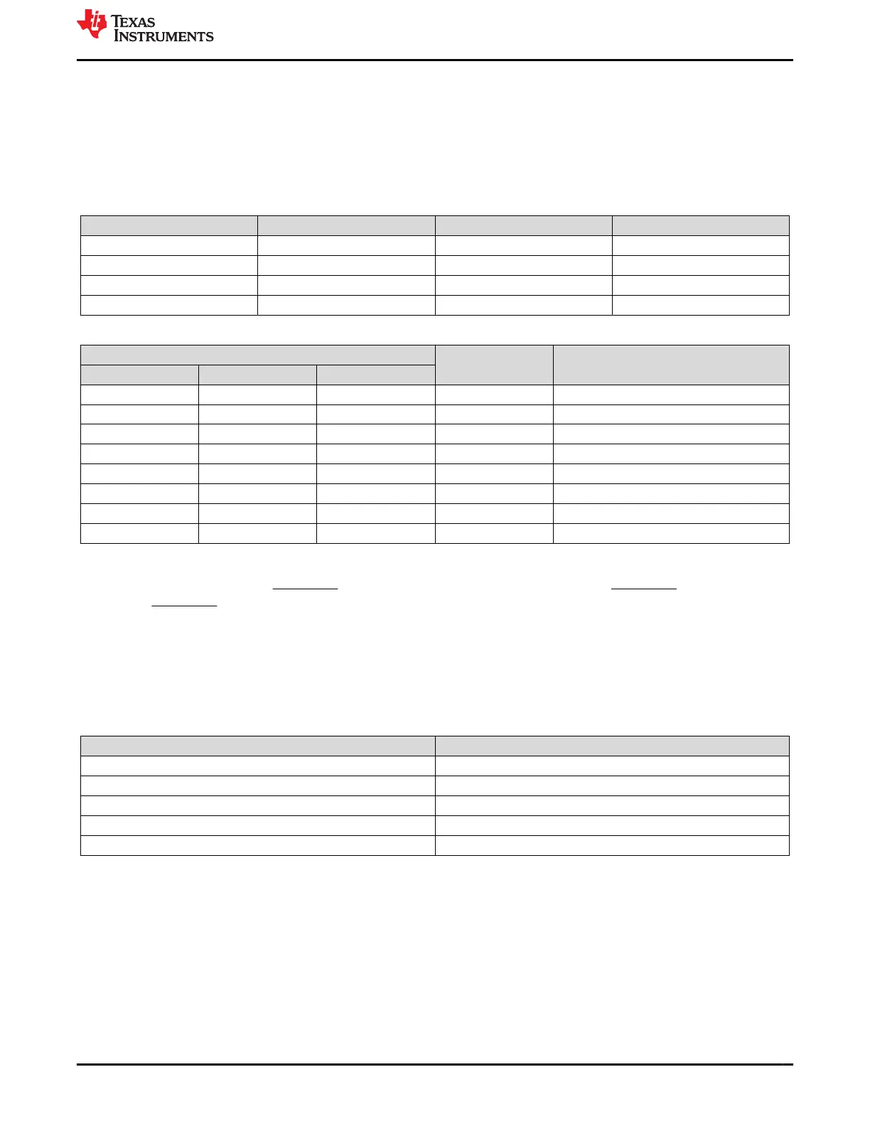
Table 2-1 details which resistor pads correspond to which ADCIN switch set and jumper.
Table 2-1. ADCIN Inputs for Jumpers
Jumper ADCIN Input Pull-up resistor Pull-down resistor
J8 ADCIN1 R22 R30
J7 ADCIN2 R23 R31
J6 ADCIN3 R24 R32
J5 ADCIN4 R25 R33
Table 2-2. Decoding of ADCINx Pins
DIV = R
DOWN
/ (R
UP
+ R
DOWN
)
Without Using R
UP
or R
DOWN
ADCINx Decoded Value
MIN Target MAX
0 0.0114 0.0228 tie to GND 0
0.0229 0.0475 0.0722 N/A 1
0.0723 0.1074 0.1425 N/A 2
0.1425 0.1899 0.2372 N/A 3
0.2373 0.3022 0.3671 N/A 4
0.3672 0.5368 0.7064 tie to LDO_1V5 5
0.7065 0.8062 0.9060 N/A 6
0.9061 0.9530 1.0 tie to LDO_3V3 7
2.4 Push Buttons
Push button SW5 controls the FAULT_IN GPIO input. Pressing the SW5 button sets FAULT_IN to logical high.
The use of FAULT_IN is detailed in the TPS25730 data sheet (SLVSGP9).
2.5 Debug Information
2.6 Test Points
The test points available are as follows:
Table 2-3. TPS25730EVM Test Points
Test Point Pin
TP1 VIN_3V3
TP2 LDO_3V3
TP3 LDO_1V5
TP4 CC1
TP5 CC2
www.ti.com Hardware
SLVUCP4 – NOVEMBER 2023
Submit Document Feedback
TPS25730 Evaluation Module 5
Copyright © 2023 Texas Instruments Incorporated