Time (10 Ps/div)
Current (A)
Voltage (V)
-5 -5
0 0
5 5
10 10
15 15
20 20
25 25
30 30
D007
I VBUS
VBUS
PP_HV
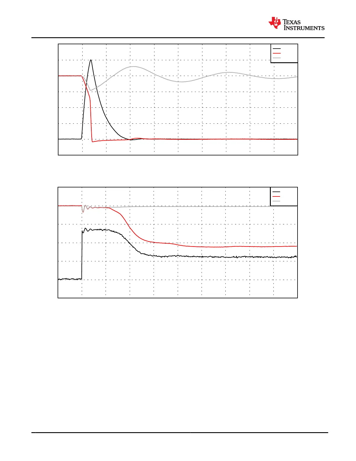
Figure 9-18. PP_HV Current Limit Response with a Hard Short
Time (200 Ps/div)
Current (A)
Voltage (V)
-1 -5
0 0
1 5
2 10
3 15
4 20
5 25
D008
I VBUS
VBUS
PP_HV
Figure 9-19. PP_HV Current Limit Response with a Soft Short (7 Ω)
9.3.3.10 External HV Power Delivery
The TPS65982 is capable of controlling an external high-voltage, common-drain back-to-back NMOS FET switch
path to source or sink power up to the maximum limit of the USB PD specification: 20 V at 5 A of current. The
TPS65982 provides external control and sense to external NMOS power switches for currents greater than 3
A. This path is bi-directional for either sourcing current to VBUS or sinking current from VBUS. The external
NMOS switches are back-to-back to protect the system from large voltage differential across the FETs as well as
blocking reverse current flow. Each NFET has a separate gate control. HV_GATE2 is always connected to the
VBUS side and HV_GATE1 is always connected to the opposite side, referred to as PP_EXT. Two sense pins,
SENSEP and SENSEN, are used to implement reverse current blocking, over-current protection, and current
sensing. The external path may be used in conjunction with the internal path. For example, the internal path
may be used to source current from PP_HV to VBUS when the TPS65982 is acting as a power source and the
external path may be used to sink current from VBUS to PP_EXT to charge a battery when the TPS65982 is
acting as a sink. The internal and external paths must never be used in parallel to source current at the same
TPS65982
SLVSD02E – MARCH 2015 – REVISED AUGUST 2021
www.ti.com
44 Submit Document Feedback
Copyright © 2021 Texas Instruments Incorporated
Product Folder Links: TPS65982