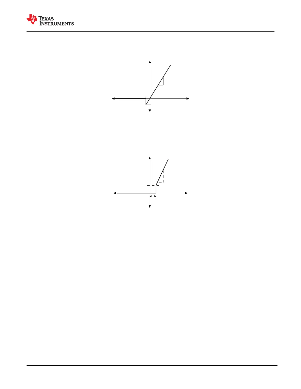
calculated by Equation 3 and then blocks reverse current from VBUS to PP_HV. Figure 9-16 shows the diode
behavior of the switch as a source.
IREVHV = VREVHV/RPPHV
(3)
Figure 9-16. Internal HV Switch I-V Curve as a Source
9.3.3.7 Internal HV Power Switch as a Sink
The TPS65982 can also receive power from VBUS to PP_HV when operating as a sink. When the switch is on
as a sink the path behaves as an ideal diode and blocks reverse current from PP_HV to VBUS. Figure 9-17
shows the diode behavior of the switch as a sink.
VREVHV
I
VBUS-PP_HV
1/RPPHV
VREVHV/RPPHV
Figure 9-17. Internal HV Switch I-V Curve as a Sink
9.3.3.8 Internal HV Power Switch Current Sense
The current from PP_HV to VBUS is sensed through the switch and is available to be read digitally through the
ADC only when the switch is sourcing power. When sinking power, the readout from the ADC will not reflect the
current.
9.3.3.9 Internal HV Power Switch Current Limit
The current through PP_HV to VBUS is current limited to ILIMPPHV (only when operating as a source) and
is controlled automatically by the digital core. When the current exceeds ILIMPPHV, the current-limit circuit
activates. Depending on the severity of the over-current condition, the transient response will react in one of two
ways: Figure 9-18 shows the approximate response time and clamping characteristics of the circuit for a hard
short while Figure 9-19 shows the approximate response time and clamping characteristics for a soft short of 7
Ω.
www.ti.com
TPS65982
SLVSD02E – MARCH 2015 – REVISED AUGUST 2021
Copyright © 2021 Texas Instruments Incorporated
Submit Document Feedback
43
Product Folder Links: TPS65982