Figure 12-2. Under Ball Recommended Via Size
12.1.2 Alternate TPS65982 Footprint (Oval Pads)
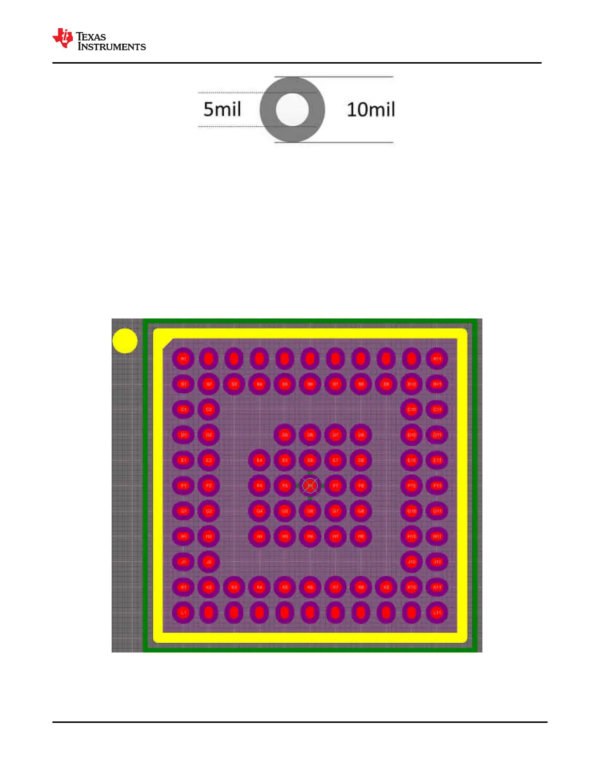
Figure 12-3 shows the TPS65982 footprint using oval-shaped pads in specific locations. This allows the PCB
designer to route the inner perimeter balls through the top layer. The balls around the perimeter have their
pads in an oval shape with the exception of the corner balls. Figure 12-4 shows the sizing for the oval pads,
0.25 mm by 0.17 mm. All of the other non-oval shaped pads will have a 0.25 mm diameter. This footprint is
recommended for MDI (Medium Density) PCB designs that are generally less expensive to build. The void under
the TPS65982 allows for vias to route the inner signals and connect to the GND and power planes. Figure 12-5
shows the recommended minimum via size (8mil hole and 16 mil diameter). The recommended 8mil vias will be
rated for approximately 1.8 A of DC current and 1.5 mΩ of resistance with 1.3 nH of inductance. Some board
manufactures may offer 6mil hole and 12 mil diameter vias with a mechanical drill. This footprint is available for
download on the TPS65982 product folder.
Figure 12-3. Top View Alternate TPS65982 Footprint (Oval Pads)
www.ti.com
TPS65982
SLVSD02E – MARCH 2015 – REVISED AUGUST 2021
Copyright © 2021 Texas Instruments Incorporated
Submit Document Feedback
93
Product Folder Links: TPS65982