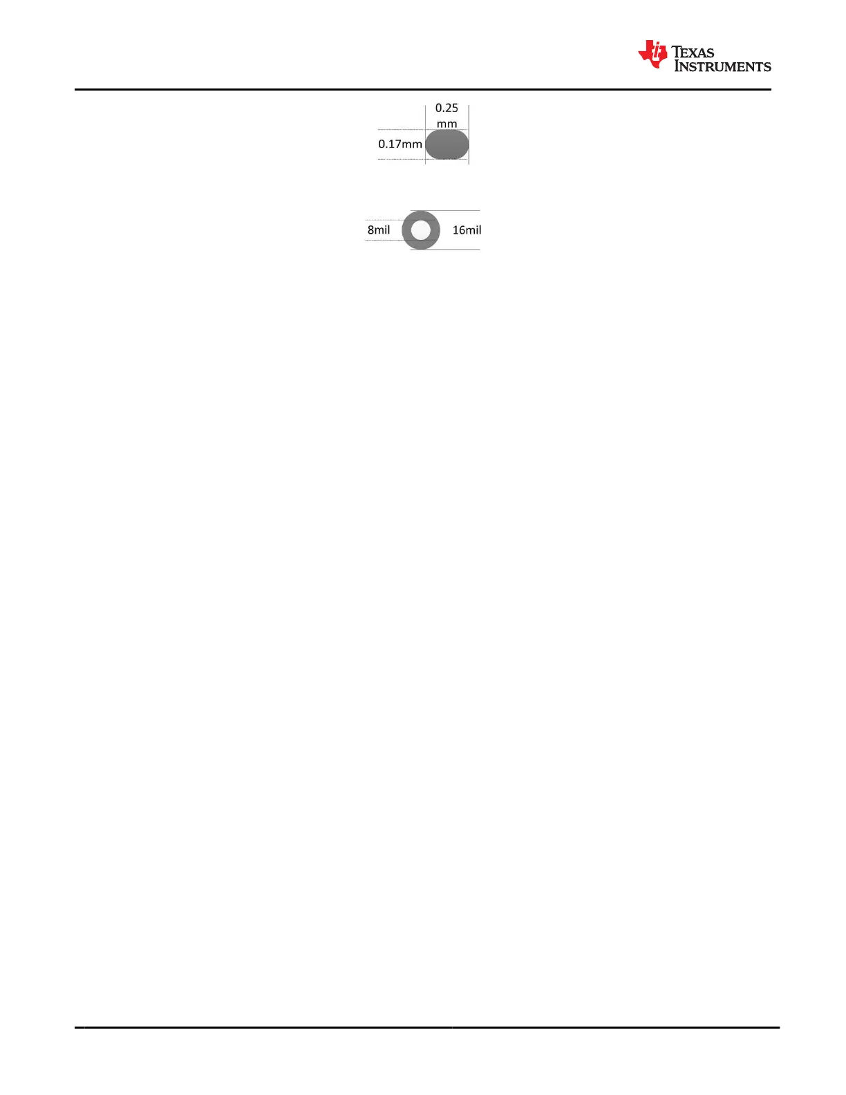
Figure 12-4. Oval Pad Sizing
Figure 12-5. Recommended Minimum Via Sizing
12.1.3 Top TPS65982 Placement and Bottom Component Placement and Layout
When the TPS65982 is placed on top and its components on bottom the solution size will be at its smallest. For
systems that do not use the optional external FET path the solution size will average less than 64 mm
2
(8 mm ×
8 mm). Systems that implement the optional external FET path will average a solution size of less than 100 mm
2
(10 mm × 10 mm). These averages will vary with component selection (NFETs, Passives, etc.). Selection of the
oval pad TPS65982 footprint or standard TPS65982 footprint will allow for similar results.
12.1.4 Oval Pad Footprint Layout and Placement
The oval pad footprint layout is generally more difficult to route than the standard footprint because of the top
layer fan-out and void via placement needed; however, when the footprint with oval pads is used, Via on Pads,
laser-drilled vias, and HDI board processes are not required. Therefore, a footprint with oval pads is ideal for
cost-optimized applications and will be used for the following the layout example. This layout example follows the
charger application example (see Typical Applications) and includes all necessary passive components needed
for this application. This design uses both the internal and optional external FET paths for sourcing and sinking
power respectively. Follow the differential impedances for High Speed signals defined by their specifications
(DisplayPort - AUXN/P and USB2.0). All I/O will be fanned out to provide an example for routing out all pins, not
all designs will use all of the I/O on the TPS65982.
12.1.5 Component Placement
Placement of components on the top and bottom layers is used for this example to minimize solution size. The
TPS65982 is placed on the top layer of the board and the majority of its components are placed on the bottom
layer. When placing the components on the bottom layer, it is recommended that they are placed directly under
the TPS65982 in a manner where the pads of the components are not directly under the void on the top layer.
Figure 12-6 and Figure 12-7 show the placement in 2-D. Figure 12-8 and Figure 12-9 show the placement in
3-D.
12.1.6 Designs Rules and Guidance
When starting to route nets it is best to start with 4 mil clearance spacing. The designer may have to adjust the
4mil clearance to 3.5 mil when fanning out the top layer routes. With the routing of the top layer having a tight
clearance, it is recommended to have the layout grid snapped to 1 mil. For certain routes on the layout done in
this guide, the grid snap was set to 0.1 mil. For component spacing this design used 20 mil clearance between
components. The silk screen around certain passive components may be deleted to allow for closer placement
of components.
12.1.7 Routing PP_HV, PP_EXT, PP_5V0, and VBUS
On the top layer, create pours for PP_HV, PP_5V0 and VBUS to extend area to place 8 mil hole and 16 mil
diameter vias to connect to the bottom layer. A minimum of 4 vias is needed to connect between the top and
bottom layer. For the bottom layer, place pours that will connect the PP_HV, PP_5V0, and VBUS capacitors to
their respective vias. The external FETS must also be connected through pours and place vias for the external
FET gates. For 5 A systems, special consideration must be taken for ensuring enough copper is used to handle
the higher current. For 0.5 oz copper top or bottom pours with 0.5-oz plating will require approximately a 120-mil
pour width for 5-A support. When routing the 5 A through a 0.5 oz internal layer, more than 200 mil will be
required to carry the current. Figure 12-10 and Figure 12-11 show the pours used in this example.
TPS65982
SLVSD02E – MARCH 2015 – REVISED AUGUST 2021
www.ti.com
94 Submit Document Feedback
Copyright © 2021 Texas Instruments Incorporated
Product Folder Links: TPS65982