12.1.8 Routing Top and Bottom Passive Components
The next step is to route the connections to the passive components on the top and bottom layers. For the top
layer only CC1 and CC2 capacitors will be placed on top. Routing the CC1 and CC2 lines with a 8 mil trace will
facilitate the needed current for supporting powered Type C cables through VCONN. For more information on
VCONN please refer to the Type C specification. Figure 12-12 shows how to route to the CC1 and CC2 to their
respective capacitors. For capacitor GND pin use a 10 mil trace if possible. This particular system support Dead
Battery, which has RPD_G1/2 connected to CC1/2.
The top layer pads will have to be connected the bottom placed component through Vias (8 mil hole and 16
mil diameter recommended). For the VIN_3V3, VDDIO, LDO_3V3, LDO_1V8A, LDO1V8D, LDO_BMC, and
VOUT_3V3 use 6mil traces to route. For PP_CABLE route using an 8 mil trace and for all other routes 4 mil
traces may be used. To allow for additional space for routing, stagger the component vias to leave room for
routing other signal nets. Figure 12-13 and Figure 12-14 show the top and bottom routing. Table 12-1 provides a
summary of the trace widths.
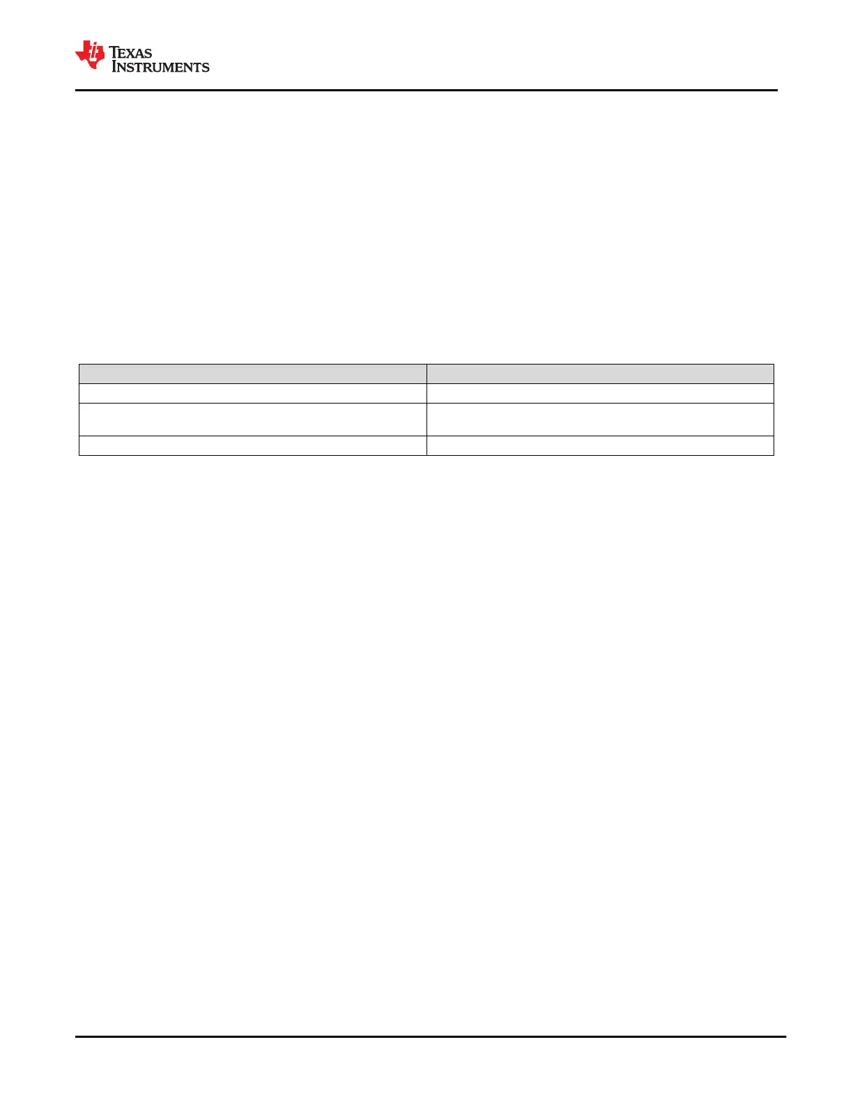
Table 12-1. Routing Trace Widths
ROUTE WIDTH (mil)
CC1, CC2, PP_CABLE 8
LDO_3V3, LDO_1V8A, LDO_1V8D, LDO_BMC, VIN_3V3,
VOUT_3V3, VDDIO, HV_GATE1, HV_GATE2
6
Component GND 10
12.1.9 Void Via Placement
The void under the TPS65982 is used to via out I/O and for thermal relief vias. A minimum of 6 vias must be
used for thermal dissipation to the GND planes. The thermal relief vias must be placed on the right side of the
device by the power path. Figure 12-15 shows the recommended placement of the vias. Note the areas under
the void where vias are not placed. This is done to allow the external FET gate drive and sense pins to route
under the TPS65982 through an inner layer. Figure 12-16 shows the top layer GND pour to connect the vias and
GND balls together.
12.1.10 Top Layer Routing
Once the components are routed, the rest of the area can be used to route all of the additional I/O. After all nets
have been routed place a polygonal pour under to connect the TPS65982 GND pins to the GND vias. Refer to
Figure 12-17 for the final top routing and GND pour.
12.1.11 Inner Signal Layer Routing
The inner signal layer is used to route the I/O from the internal balls of the TPS65982 and the external FET
control and sensing. Figure 12-18 shows how to route the internal layer.
12.1.12 Bottom Layer Routing
The bottom layer has most of the components placed and routed already. Place a polygon pour to connect all of
the GND nets and vias on the bottom layer, refer to Figure 12-19.
www.ti.com
TPS65982
SLVSD02E – MARCH 2015 – REVISED AUGUST 2021
Copyright © 2021 Texas Instruments Incorporated
Submit Document Feedback
95
Product Folder Links: TPS65982