70
Analog Front End IC TMS37122 - Reference Guide August ’01
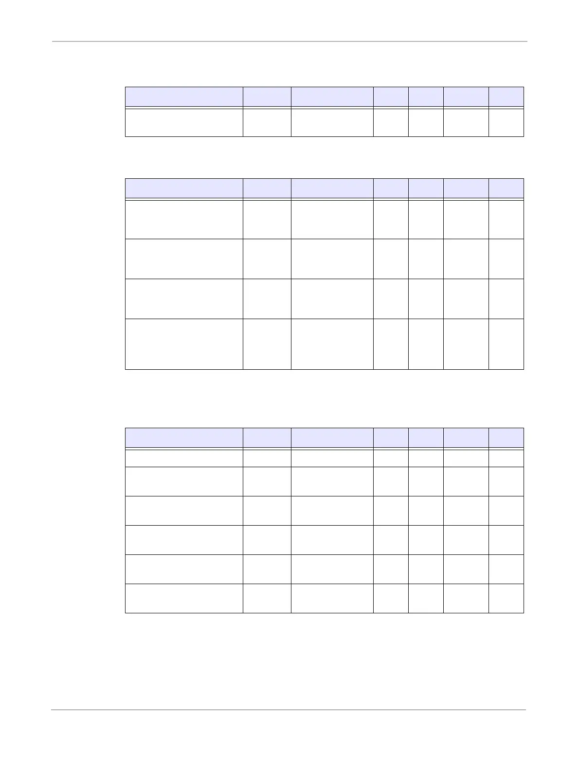
4.2.4.12 CLKA Sensitivity
4.2.4.13 EOBA Sensitivity
Note 1: a= Vmin / Vmax = (1-m) / (1+m)
4.2.4.14 AGC Amplifier
Parameter Sign Note Min Nom Max Unit
Clock Regenerator
Sensitivity, CLKA
Vclka
VWakeA/
2
mVpp
Parameter Sign Note Min Nom Max Unit
Modulation Depth for valid
EOBA
m
Vmax=
VwakeA,
Note1
33
(a=50%)
%
Modulation Depth for idle
EOBA
m(idle)
Vmax=VwakeA,
Note 1
2
(a=
96%)
EOBA Activation Delay dtEOBA
VRF = VWAKE to
VWAKE/2,
VBAT=2V
15 46 90 µs
EOB Deactivation Delay dtNEOB
Step VRF =
VWAKE/2 to
VWAKE,
VBAT=2V
15 42 60 µs
Parameter Sign Note Min Nom Max Unit
Coupling Capacity Ccpl 1 pF
Input Impedance/ Low
Amplitude
Rin
Vrf=5mVpp,
fTX= 134.2kHz
2MΩ
Input Impedance/ High
Amplitude
Rin
Vrf=15Vpp,
fTX=134.2 kHz
1.2 MΩ
Center frequency of
amplifier
fc_AGC 120 kHz
-3dB Band-width of amplifier
dfAGC
-3dB
50 kHz
-20dB Band-width of
amplifier
dfAGC
-20dB
270 kHz