Symbol
V
DS
V
GS
I
DM
T
J
, T
STG
Symbol Typ Max
33 40
62 75
R
θJL
18 24
W
Maximum Junction-to-Lead
C
Steady-State
°C/W
Thermal Characteristics
Parameter Units
Maximum Junction-to-Ambient
t ≤ 10s
R
θJA
°C/W
Maximum Junction-to-Ambient
Steady-State
°C/W
±20Gate-Source Voltage
Drain-Source Voltage -30
Continuous Drain
Current
A
Maximum UnitsParameter
T
A
=25°C
T
A
=70°C
Absolute Maximum Ratings T
A
=25°C unless otherwise noted
V
V
-5.3
-30
Pulsed Drain Current
B
Power Dissipation
A
T
A
=25°C
Junction and Storage Temperature Range
A
P
D
°C
3.1
2
-55 to 150
T
A
=70°C
I
D
-6.5
AO4459
P-Channel Enhancement Mode Field Effect Transistor
Features
V
DS
(V) = -30V
I
D
= -6.5A (V
GS
= -10V)
R
DS(ON)
< 46mΩ (V
GS
= -10V)
R
DS(ON)
< 72mΩ (V
GS
= -4.5V)
General Description
The AO4459 uses advanced trench technology to provide
excellent R
DS(ON)
with
low gate charge. This device is suitable
for use as a load switch or in PWM applications. Standard
roduct AO4459 is Pb-free (meets ROHS & Sony 259
specifications). AO4459L is a Green Product ordering
option. AO4459 and AO4459L are electrically identical.
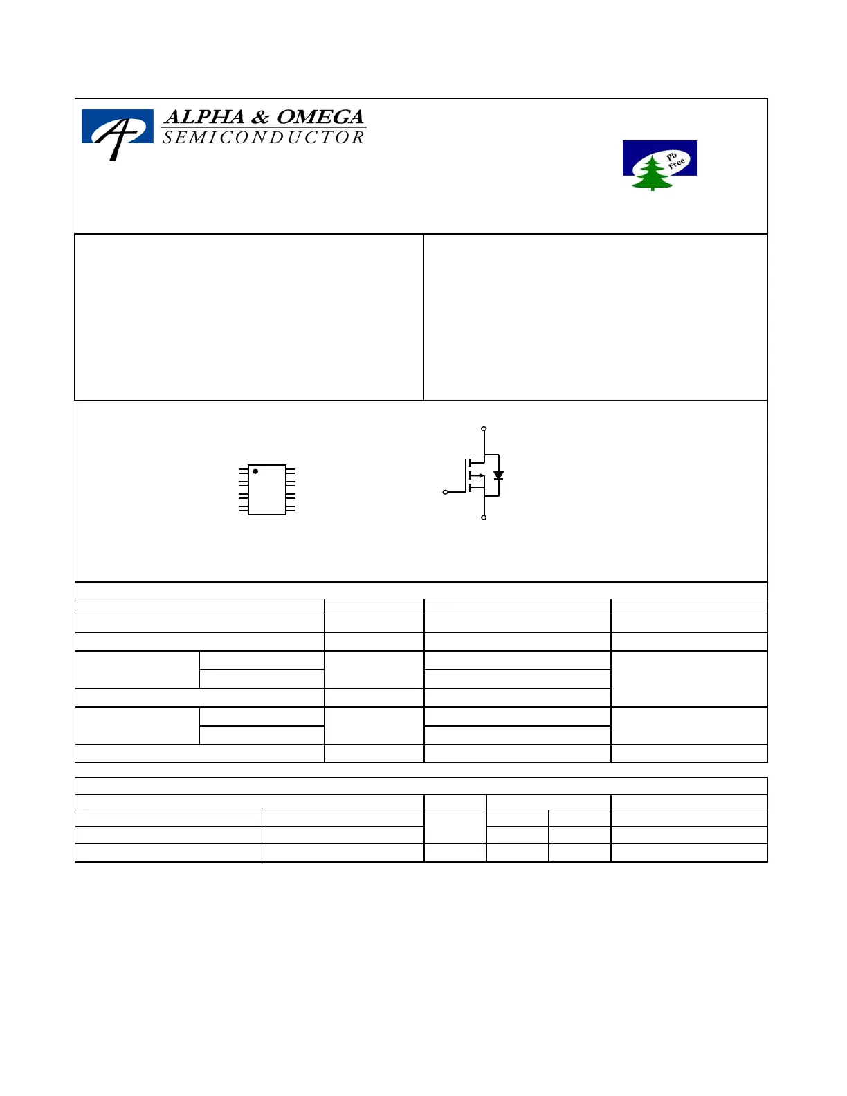
G
D
S
SOIC-8
Top View
G
S
S
S
D
D
D
D
Alpha & Omega Semiconductor, Ltd.