PCM30U, PCM30U-OCH – User's, Operating and Maintenance Manual
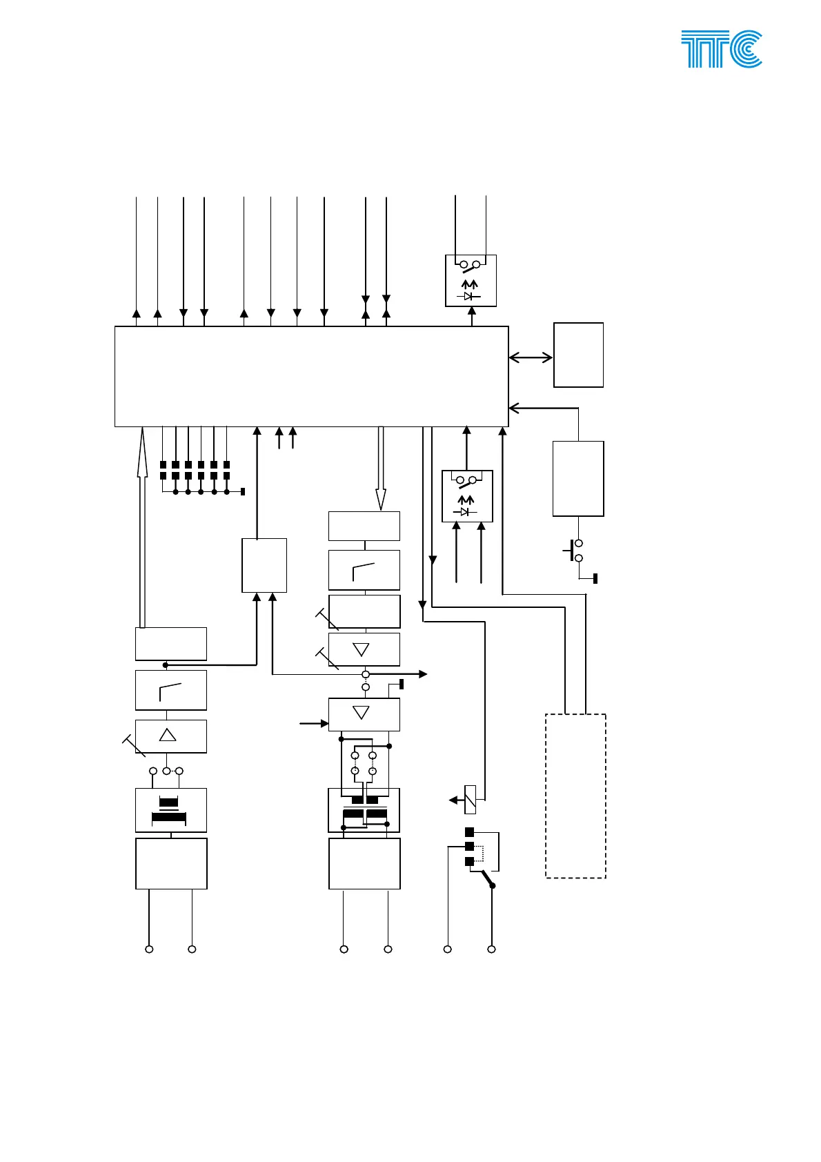
E.2.3 Block diagram
+
Σ ERR
-
ZK
Feedback
check
IN1A
IN1B
U1- 50 Hz
U2- 50 Hz
OUT1A
OUT1B
overvoltage
protection
T100
T101
A1
1
3
UB=-48V
OFF1+
A3
XJ104
ERR1+
ERR1-
KH100
XJ106
A2 LP2
2,8kHz
Phase
correct
ion
D/A
LP1
2,8kHz
A/D
10 bit samples from 1
st
channel
Note:
+) Failure condition of the contacts of the KH100 relay
(no current supplied to the coil of the relay)
2
XJ102
PLD-XILINX
Microcontroller
1
8
XJ1- HW
mode
configuration
10 bit
Transmitting BUS M1
Receiving BUS M1
SKIM
TAKT 2048 kHz
SYNN 500 Hz
Position in subrack
Program
memory
WATCHDOG
SW3
RESET
on panel
+5 V
2
n
channel RO4
Management IP
XJ103
overvoltage
protection
OFF1
OFF1-
OFF2
ERR1
ERR2
OFF2
-48V
RP101
GAIN 1
RP102
± φ 1
RP100
XJ105
XJ300 –
Parallel operation
with2
nd
channel
SW1/2
Digital delay
switch on panel
+ms 1 / 2
Management SK
Transmitting BUS M2
Receiving BUS M2
3 2
1
Fig 4 Block diagram of the RO4 unit (one channel)
Power Channel Modules E-33 446S037.914.14N00