ZED-F9P-Integration Manual
UBX-18010802 - R01
5 Design Page 52 of 64
Objective Specification - Confidential
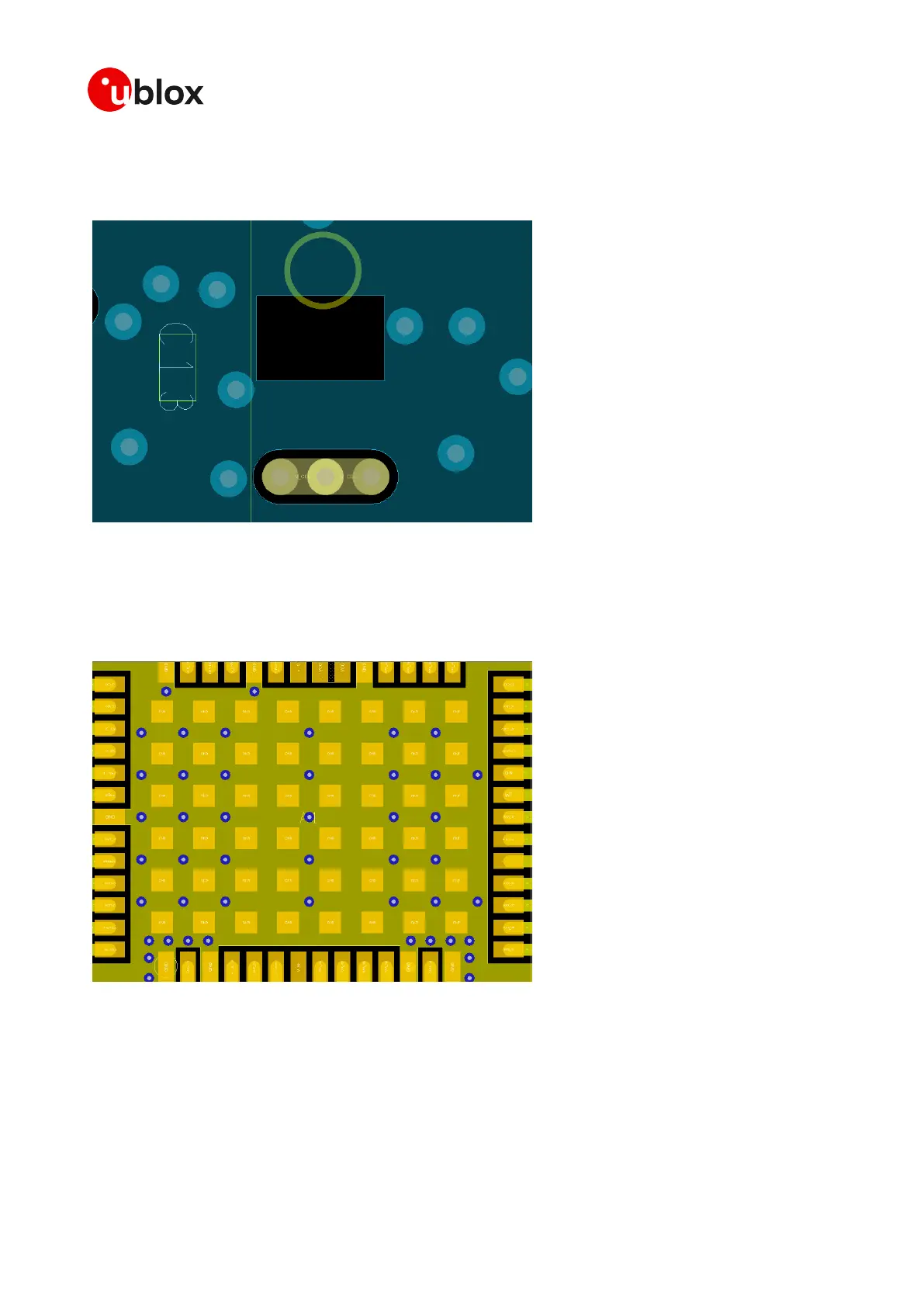
The RF in trace on the Top layer should be referenced to Layer 2 (Ground). However the ZED-F9P
high precision receiver RF IN pad should have a slot surrounding it in the layer 2 Ground layer as
shown below.
Figure 52: Layer 2 Ground
5.6.2 Vias for the ground pads
The ground pads under the ZED-F9P high precision receiver need to be grounded with vias to the
lower ground layer of the PCB. A solid ground layer fill on the Top layer of the PCB is recommended.
This is shown in the figure below.
Figure 53: Top layer fill and vias
5.6.3 VCC pads
The VCC pads for the ZED-F9P high precision receiver need to be as low an impedance as possible
with large vias to the lower Power layer of the PCB. The VCC pads need a large combined pad and
the de-coupling capacitors must be placed as close as possible. This is shown in the figure below.
 Loading...