______________
side). Then type in the address, the cursor will blink at the address specified in the space marked new
address.
For ROM you can input 0—F. And for PLD you only could input 0 and 1.
WARNING! Input address must not overlap.
6.1.3 Data Edit
This selection brings up the Fuse Buffer edit windows if the device type is a PLD, or the Data Buffer edit
window for memory devices. The buffer is for 8-bit data, and the numbers in the left column are the
addresses of the buffer.
For the Fuse Buffer edit window, 1 is logic High and 0 is logic Low.
The Data Buffer edit window has two edit areas: one supports Hex code, and the other supports ASCII.
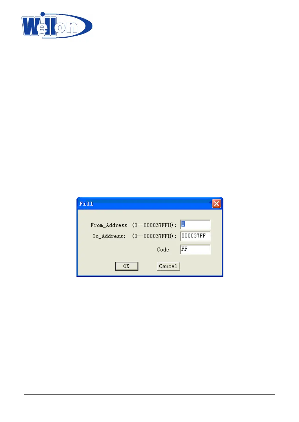
6.1.4 Fill
This selection will bring up the Fill buffer dialogue box. It consists of the Start address input line, End address
input line, Fill data input line, OK and Cancel buttons. Input any desired data to be filled into the Fill data input
line, and specify the range by indicating the beginning and ending addresses. For the Fuse buffer edit
window, the data will be either 1 or 0.For the Data buffer edit window, it will be a two-character HEX code.
6.1.5 Copy
This selection displays the Copy buffer dialogue box. It consists of the Start address input line, End address
input line, new address input line, OK and Cancel buttons. Data between Start address and End address will
be copied to the buffer starting from New address.
Note that the source and destination area must not overlap.
Tianjin Weilei Techonlogy Ltd.
www.weilei.com TEL:022-83945122
FAX:022-83945121 2018-03-08